The schematic for the ZX81 Module I designed in2016 had been designed in a very old version of KiCad, and hadn’t survived all the upgrades too well. This resulted in every component being replaced by a question mark in a box. Luckily I had some photos of the schematic from previous Retro Challenge posts, as well as an expectation as to what should be resistors or capacitors or whatever.

Things now look much better, and actually make some kind of sense.
2016 Me didn’t consider the importance of putting component values on the schematic. Or the PCB. My module was based on the original ZX81 schematic though, so it was pretty much a case of matching up components and updating their values.
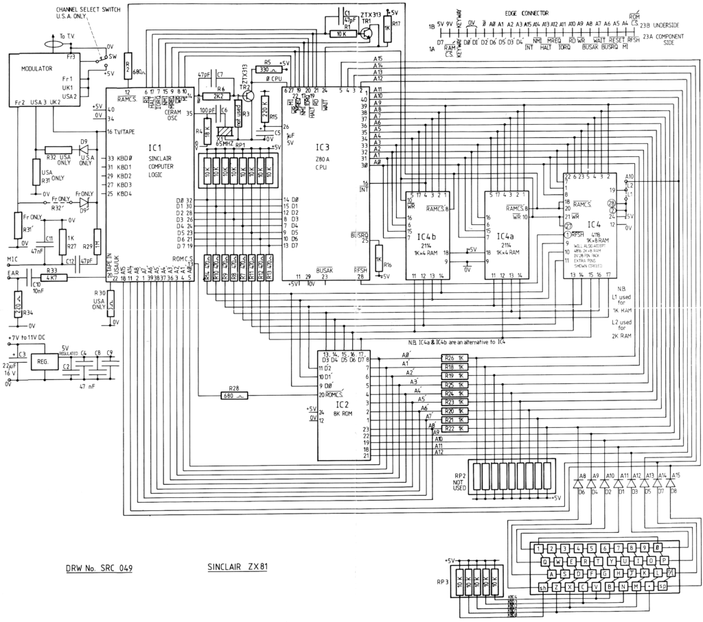
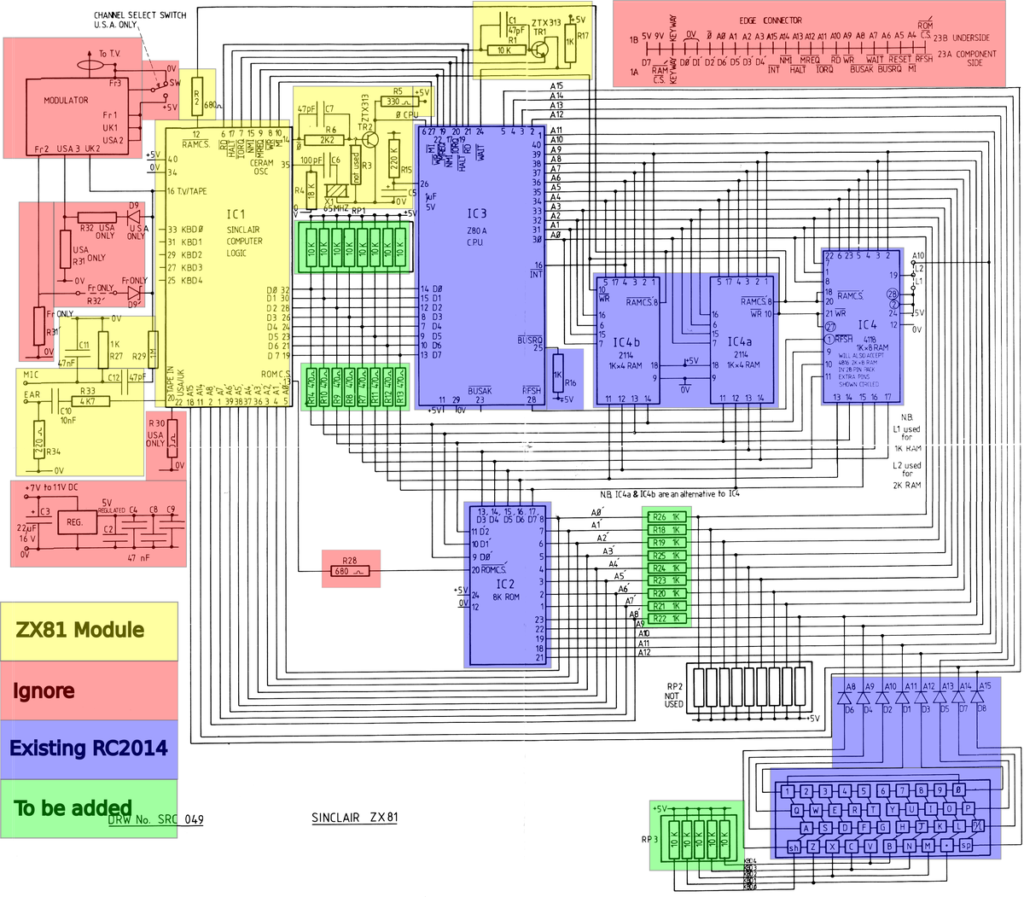
The observant amongst you will notice that the ZX81 schematic has a lot more stuff on it than my module. These changes can be categorised in three ways;
- Components which the RC2014 already have, such as the Z80 CPU, ROM or RAM
- Components which need to be added, but are not part of the module, such as the keyboard or data/address bus resistors
- Components which will not need to be included, such as the TV modulator including the USA/French options, or power regulation.
In addition, I noticed my module design had some extra components that were not part of the ZX81 schematic.

More specifically, this is a transistor and resistor. This actually matches the composite mod that the donor machine had. So, well done 2016 me for thinking ahead and including this!
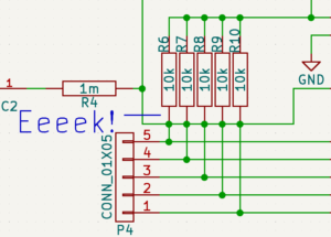
Something which is a bit more concerning though is the way that the keyboard lines all seem to be shorted against the TV Out netlist. I think this might be an artifact of the schematic rescue, as I am sure that 2016 Me would have noticed that. However, I still need to test the PCB in case this fault has made its way through to the board.
So, with a donor ULA, and all the component values, I have everything I need to finish the module. There are other important things that I need to do to the RC2014 though. Firstly, I need to burn a ROM.
You may remember from a recent post that I did a partial ROM dump from the donor machine. This was a simple BASIC program
10 FOR F=1 TO 200
20 PRINT PEEK F;
30 NEXT F
I remember reading that the ROM chips used on old machines were almost, but not identical pin out to the 27C EPROM chips, and that it was a couple of data pins which were swapped over. Or something like that. So my worry was that, for example, D3 and D7 on every byte was swapped. So if I could compare the first 200 bytes or so then I would know if everything matched, or if the difference was consistent.
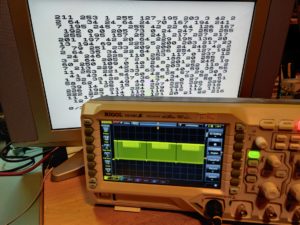
Luckily, everything matched with the ZX81.ROM file I have.
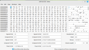
Although converting decimal to hex becomes less and less fun as you go. But at least I know that I should be able to just burn that image to a ROM and it *should* work.
The memory map on a ZX81 is a ZX81 is interesting. The ROM shows up in 4 locations, and the RAM is mirrored too. A13 is the only line used to decode if ROM or RAM is accessed. Therefor the memory map looks like this;
FFFF
      RAM (Shaddow)
E000
DFFF
      RAM (Shaddow)
C000
BFFF
      ROM (Shaddow)
A000
9FFF
      ROM (Shaddow)
8000
7FFF
      RAM
6000
5FFF
      RAM
4000
3FFF
      ROM (Shaddow)
2000
1FFF
      ROM
0000
As I understand it, Only the 8 ROM from 0x000 to 0x1FFF and the 16k RAM from 0x4000 to 0x7FFF actually matter. However, my plan is to burn two consecutive copies of the ROM and set the Pageable ROM Module to a 16k bank size. I will also use a 64k RAM Module with RAM starting at 0x4000. This will mean that the shaddow ROMs from 0x8000-0xBFFF will actually be RAM. I very much doubt that anything makes calls to that address range expecting it to be ROM, but as long as it isn’t critical to bootup, I can write a routing to fill that RAM with the ROM contents.
So, with all of that sorted out… I just need to solder some components, burn a ROM, and put it all together.
