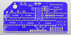
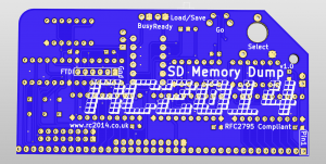
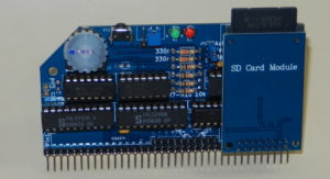
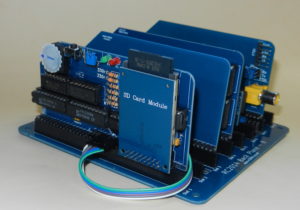
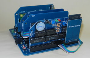
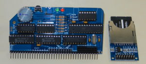
The SD Memory Dump Module is a way to either dump the memory of the RC2014 to a file on SD card, or to dump the contents of a file on SD card to the RC2014 memory. Whilst it can easily be used with a regular RC2014 with 8k ROM and 32k RAM, it supports the full 64k of address space and can therefore be used with a ROMless 64k RAM RC2014 and is particularly useful for development of new ROM images.
In order to reduce complexity and cost, the brains of the SD Dump Module comprises of an ATMEGA328 (ie Arduino) and a generic Chinese SD card module. It takes advantage of the BUSACK and BUSREQ pins on the enhanced RC2014 bus, although as the backplane to support this is not currently available, it needs a couple of jumper cables running back to those pins on the CPU Module.
Please note that whilst this is functional, the firmware is currently at a very early stage.
Save
If the Load/Save jumper is in the Save position when Go is pushed, the sequence of events runs as follows;
- The NOR gate latch connected to the BUSREQ line causes the line to go low
- When the CPU has finished it’s current instruction, it releases control of the bus
- The CPU sets the BUSACK line low to acknowledge that it has relinquished control
- The low BUSACK signal enables 3 74LS245 buffers
- The low BUSACK signal also pulls pin 2 of the ATMEGA328 low, thus triggering the Load/Save routine
- The ‘328 checks pin 23 (WRREQ) to see the state of the Load/Save switch. If high, the Save procedure is executed
- A file on the SD card* is opened to be saved to
- The ‘328 sends a Count Reset signal to the 4 4bit counters
- The 4 4bit counters are connected via the buffer to the address bus, thus the address is set to 0x0000
- The RD pin is held low by the Load/Save switch
- The ‘328 reads the 8 pins connected to the data bus and saves the byte to a file on the SD Card*
- The ‘328 sends a Count pulse to the first of the 4 4bit counters, thus incrementing the address to 0x0001
- Another read of the data bus occurs and the next byte is saved to the SD card.
- The counters are daisy-chained, so everytime the Count pin on the ‘328 is pulsed it will count up until it reaches 0xFFFF
- Once the ‘328 has sent 65536 Count pulses (ie read the entire 64k address range), the file is closed.
- The ‘328 sends a Done pulse on pin 25. This resets the latch, which takes the BUSREQ back to high.
- Optionally, the Done pulse can do an automatic reset of the Z80, so a warm reset will put it back in to a known good state.
- The Z80 will take the BUSACK line high again and take control of the bus again.
Load
If the Load/Save jumper is in the Load position when Go is pushed, the sequence of events runs as follows;
- The NOR gate latch connected to the BUSREQ line causes the line to go low
- When the CPU has finished it’s current instruction, it releases control of the bus
- The CPU sets the BUSACK line low to acknowledge that it has relinquished control
- The low BUSACK signal enables 3 74LS245 buffers
- The low BUSACK signal also pulls pin 2 of the ATMEGA328 low, thus triggering the Load/Save routine
- The ‘328 checks pin 23 (WRREQ) to see the state of the Load/Save switch. If low, the Load procedure is executed
- A file on the SD card* is opened to be read from
- The 8 pins on the ‘328 connected to the data bus are set to outputs
- The ‘328 sends a Count Reset signal to the 4 4bit counters
- The 4 4bit counters are connected via the buffer to the address bus, thus the address is set to 0x0000
- The first byte in the selected file is read
- The 8 pins connected to the data bus are set according to the byte that’s been read
- The WR pin is toggled by pin 23 (WRToggle) of the ‘328
- The ‘328 sends a Count pulse to the first of the 4 4bit counters, thus incrementing the address to 0x0001
- Another read of the SD card occurs and the next byte is put on the data bus and the WR pin is toggled.
- The counters are daisy-chained, so everytime the Count pin on the ‘328 is pulsed it will count up until it reaches 0xFFFF
- Once the ‘328 has sent 65536 Count pulses (ie read the entire 64k address range), the file is closed.
- The ‘328 sends a Done pulse on pin 25. This resets the latch, which takes the BUSREQ back to high.
- Optionally, the Done pulse can do an automatic reset of the Z80, so a warm reset will put it back in to a known good state.
- The Z80 will take the BUSACK line high again and take control of the bus again.
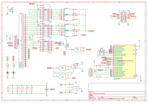
Click the schematic below for PDF
Firmware can be found on GitHub here
Note1 – an anolog pin is used as an input select. This is connected to a 10k pot as a voltage divider. Theoretically, this will give 1024 different input values, although practically, 7 would be a lot more reasonable (which would correlate to the direction of the pot pointing SW, W, NW, N, NE, E, SE). This could be interpreted as one of seven different files to load or save – although, at time of writing, this has not been implemented.
Note2 – When used in a RAM only RC2014, the RAM will be in a totally random state when powered up. The CPU starts to execute code from address 0x0000, which could be absolutely anything. Therefore, when an image is loaded in to RAM from SD card, the CPU may have already done things like set a random reset procedure and other stuff, so it is not guaranteed that this will work. Testing indicates that this is successful about 1 time in 3. Any suggestions on how to improve this are greatfully received!
Note3 – The 6 pin right angle FTDI header for programming the ‘328 must be soldered to the reverse of the PCB before the 28 pin socket is fitted. There is no jumper to isolate the power from the FTDI cable though, so either the RC2014 should be powered from the FTDI connector, or the card removed for programming, or jumper cables for Ground, Tx, Rx & RTS to be used between this module and FTDI cable.
Note4 – The Load/Save pins and jumper can be replaced with a right angle toggle or slide switch that has it’s terminals at 0.1″ pitch.
Please read the SD Memory Dump Module Safety Guide before using this module
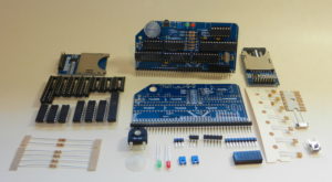
Bill of materials
1 x RC2014 SDDUMP PCB
1 x SD Card Module
1 x 40 pin RA Header
1 x 3 pin header
1 x 10 pin header
1 x 3 pin RA header
1 x 6 pin RA header
1 x 2 x 8 pin socket
2 x Jumper
1 x 28 pin narrow DIL socket
3 x 20 pin narrow DIL socket
3 x 14 pin narrow DIL socket
7 x 100nf
2 x 74LS393
1 x 74LS02
3 x 74HCT245
1 x ATMEGA328
2 x 330R resistor
4 x 10K resistor
1 x Pot 10k or greater
1 x Pot thumbwheel
1 x 3mm Green LED
1 x 3mm Red LED
1 x 16Mhz Xtal
2 x 22pf ceramic cap
1 x RA Tactile Switch

