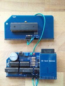
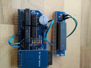
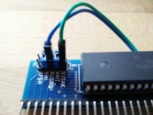
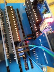
To use the SD Memory Dump Module, it must be connected to the BUSRQ and BUSACK terminals on the CPU Module. Normally the BUSRQ pin is held high at 5v either with a jumper or link, which means that the CPU has full control of the data and address bus. The SD Module goes in place of this jumper or link, and holds the BUSRQ pin high until it does a load or save. By pulling BUSRQ low it indicates to the Z80 that it wants control of the bus, which the CPU does as soon as convenient and indicates when it has done so by setting the BUSACK line low.
Version 1.0 of the CPU boards did not have these pins broken out. They are Pin 23 BUSACK and Pin 25 BUSRQ. Whilst BUSACK is easy to get to, BUSRQ will require quite a bit of PCB modification to isolate pin 25 and then reconnect all the other pins that were disconnected. See this page for more details.
Version 1.1 and 2.0 should be connected as shown below;
If both the CPU and the SD Module were to have access to the address and data bus at the same time, conflicting voltages could cause permanent damage to either device. ie if the CPU set address pin A0 low, and the SD Module set A0 high then a large amount of current would flow between the two.
The address lines on the SD Module are always high impedance (ie disconnected) unless the BUSACK pin is low. This is a safeguard against both the CPU and the SD Module from setting conflicting addresses.
The data lines on the SD Module are connected directly to the ATMEGA328, and set as input pins by the firmware. Only in a write process, which is itself triggered by the BUSACK pin going low, will the firmware set the data pins to output and write data to the address bus.
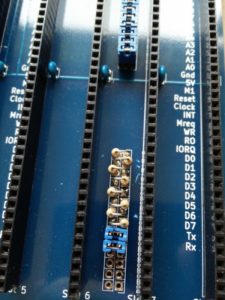
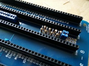
Under these conditions the SD Module is quite safe. However, connecting the BUSACK or BUSRQ lines incorrectly, or changing the firmware does pose a risk to damage occurring. To mitigate damage from bad firmware, it is recommended that a 1k resistor is fitted across each of the data lines on the backplane, either between slot 2&3 or 6&7 with the SD Module and CPU Module on different sides of the resistors, as shown below;
When programming new firmware on the SD Moudle, always remove it completely from the RC2014

