So, this is Day 2 of the Retro Challenge. In case you’re wondering what happened to Day 1, well, Day 1 happened to fall on Pub Night, therefore I was better off giving everyone else one day head start than having a go and probably putting myself back at least a week!
If you’ve read my posts on Retro Challenge so far, you’ll know my first priority is to get about half a dozen or so Printed Circuit Boards designed and sent off to the fabricators. The tool I am using to do this is KiCad, and the basic workflow is lay out the electrical circuit schematic, create a list of component, match the components up to footprints, lay the footprints out on a board, join up the various pads then create gerber (manufacturing) files.
I have decided to build my Z80 computer in a modular format, with lots of fairly basic PCBs to make up the whole thing. This should give me flexibility in how I use it and what I do with it going forward. It also makes the boards easy to design and lay out, and, if necessary, easy to troubleshoot too. So, with that in mind, I set out this evening with the goal of making the electrical schematic for at least 5 boards. Starting with the CPU board, which comprises of 1 chip, 1 connector and 1 resistor. Simples!
KiCad uses libraries of components, so when you lay out a circuit you can pick a resistor, a capacitor, voltage regulator etc. It’s got loads of chips in the default library that comes with it, but, as I discovered this evening, no Z80! I tried finding a library on line that had one, but couldn’t get anything that worked. So I had to design my own component – a 40 pin IC! Then, the connector I was going to use was for my Z80 bus, and that had my own designed layout, so that’s another 40 pin component I had to design! Luckily, a regular resistor was already available! So, join the appropriate pins up, and voila! A schematic!
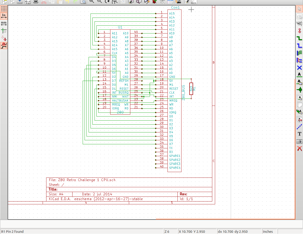
Already that was half the evening gone! So, just to make sure I was on the right track, and things actually worked as they should, I thought I’d put the first one on a board. So, I created a net list (list of all 3 components) and went to assign them footprints. The Z80 needs a 40 pin wide DIL footprint, and that’s included in the library. Great. I had a choice of a dozen or so layouts for the resistor, so that was easy. The connector though… well, although it’s only a single row of 40 holes on 0.1″ pitch (pretty standard), the largest one available was 30 pin. Ok, so I’ve got to design a footprint too. So, I create one called “40 Pin SIL” and associate it with the component. Then I lost about an hour of going around in circles, pulling my hair out, redoing stuff and swearing. Eventually, I worked out that footprint names in KiCad cannot contain spaces! Who’d have thought? So, I create another one, call it “SIL_40”, delete the old net list, and start again. Bingo!
So, off I go with laying out the PCB, and running the tracks. and end up with this;
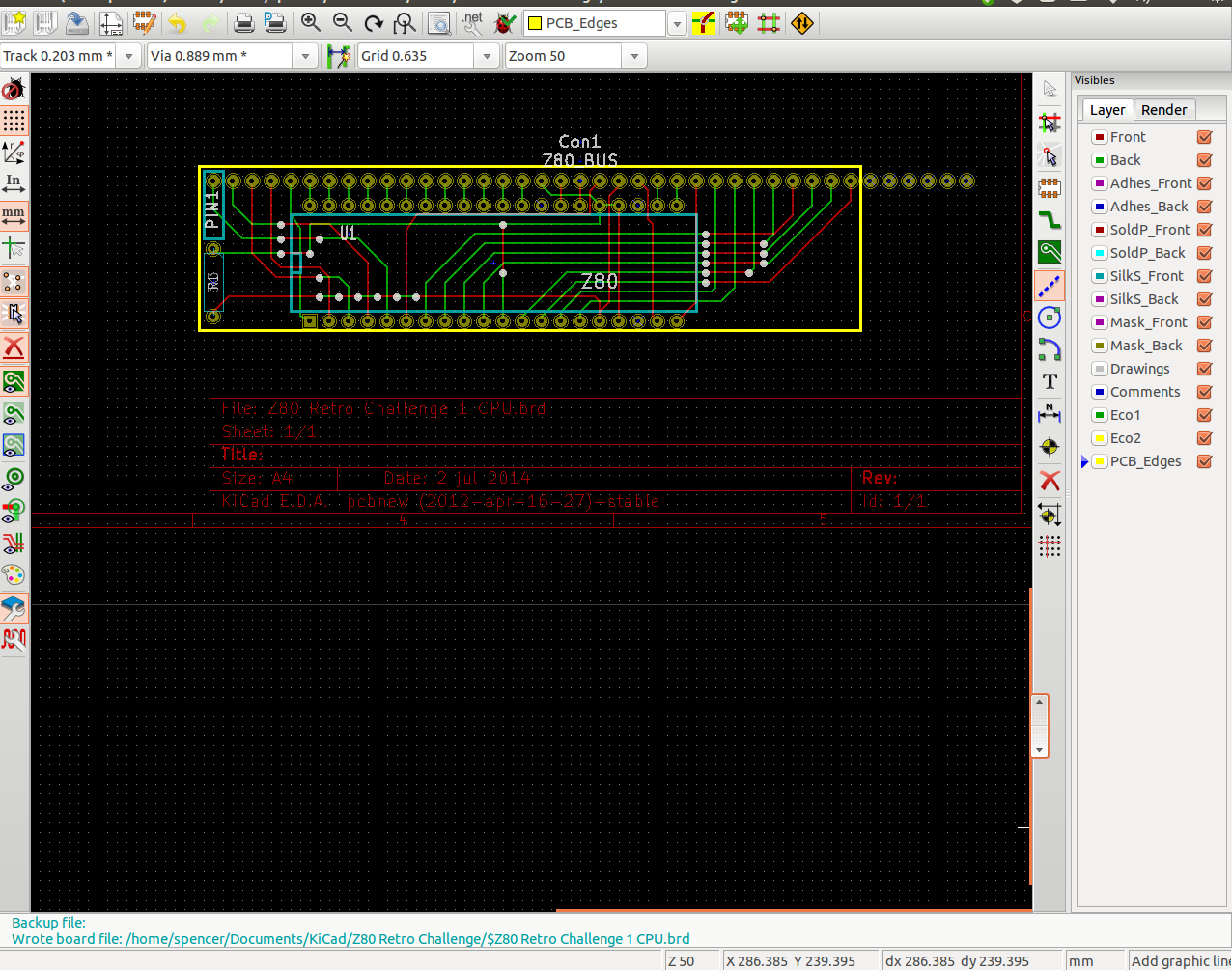
The yellow line is the actual outline of the PCB itself. You’ll notice that there’s some of the pads which are outside the board itself. As the cost of the board is based on the overall size, I’ve not extended it to cover pins that I don’t need. I know that any silk screen printing that goes outside the edge of the board is no problem, but I’ll have to wait until I create the gerber files to see if actual pads outside are a problem or not. If so, then I’ll have to create more individual footprints for other board combinations.
And all of a sudden, my whole evening has gone! One single board with 3 components isn’t much to show for almost 4 hours work, but I feel that I’ve learned a lot, and I’m much more set up to knock out a few more boards tomorrow night!