The Pageable ROM fundamentally works in a very similar way to the Switchable ROM but with a lot more selection of what size page is used and where on the ROM it is located, and also features the control circuitry to page itself out and page in the lower half of the 64k RAM Module.
[Note that the words ROM, PROM and EPROM are used interchangeably in this document. For the purposes of this module they are the same thing]
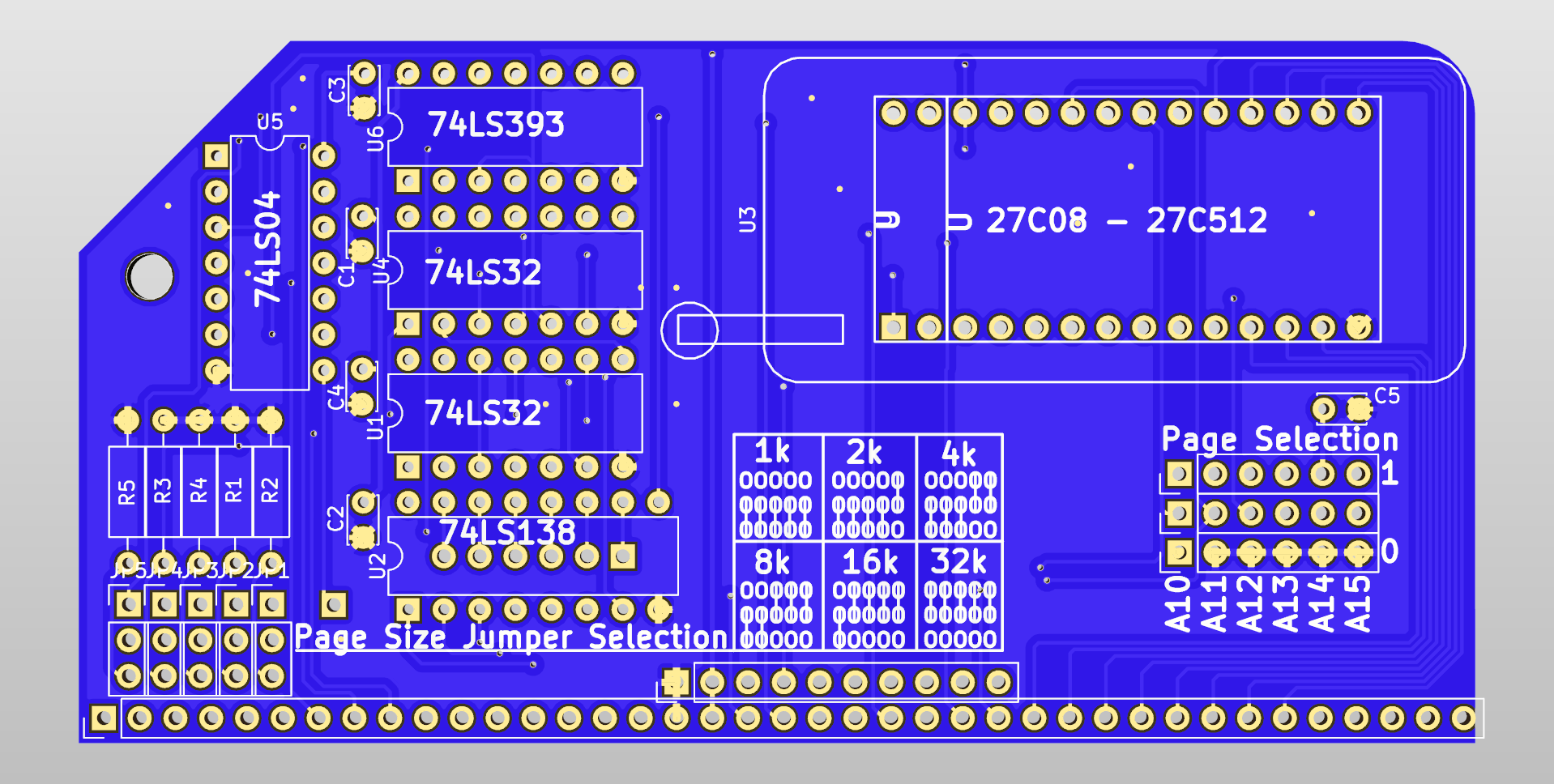
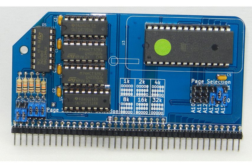
The module is designed with the 27C512 64k PROM in mind, as these are easily available and provide good value for money. However, it will work with any of the 27 series down to the 2716 (2k) size. If using a 24 pin chip, pin 1 of the chip should line up with pin 3 of the socket (ie pin 1,2,27,28 will be empty). All ROM, PROM, EPROM and EEPROM types should work fine. I believe the 28C series of chips up to 64k should also work – however, this is currently untested.

Whilst the original Swithchable ROM was hard wired for an 8k page size, this module is configurable for 1k, 2k, 4k, 8k, 16k or 32k page size – assuming you’re using a chip with sufficient capacity
The jumpers on the left select what size page is used. Here the address lines A10 – A14 from the RC2014 are either connected through to the upper address lines of the ROM or not. All address lines from A0 to A9 are conneced. If all addresses from A10 to A14 connect to A10 to A14 of the ROM then 32k is addressable. If none of A10 to A14 is connected then only 1k is addressable, and settings inbetween will give page sizes inbetween.
The jumpers on the right select where that page is located on the ROM by either pulling up or down the high address lines on the ROM. Note that depending on the size of the page some of these need to be left unjumpered. The location of this page has to be on a logical boundary for that size of page. ie a 16k page can only be at 0x0000, 0x4000, 0x8000 or 0xC000. It cannot be at 0x2000. However, a 1k, 2k, 4k or 8k page size could be at 0x2000. See the chart below

The paging is acheived by means of a 74HCT138 3 to 8 decoder and a 74LS393 counter. an OUT 0x38,n (where n can be any number) will cause the ‘138 to increment the output of the ‘393. The least significant bit of the ‘393 acts as the enable for the ROM so whenever this is low the ROM is active. Effectively, any even number on the ‘393 will enable the ROM and any odd number will disable it. This signal is also fed to the Page pin on the enhanced bus. If this is connected to the Page pin on the 64k RAM Module (instead of linking the pin as indicated on the silkscreen) then whenever the ROM is active the lower 32k of RAM isn’t and vice versa. The reset line is connected to the clear pin on the ‘393 so when the RC2014 is reset then the ROM becomes active.
The PCB has a ZIF socket footprint to allow for easy ROM insertion and removal. Note, however, that the release arm fouls two of the small ICs on the board. There are 3 ways around this, although I admit that none of them are perfect; Cut down the release arm, solder the 74LS32 direct to the PCB to lower the height or rotate the ZIF socket 180 degrees.
The source files for running CP/M can be found on Github

Bill of materials
RC2014 PAGEROM PCB 1
28 pin wide DIL socket 1
40 pin RA Header 1
3 pin header 11
10 pin header 1
Jumper 8
16 pin narrow DIL socket 1
14 pin narrow DIL socket 4
100nf 5
74LS393 1
74hct04 1
74LS32 2
74HCT138 1
10K resistor 5
RC2014 PAGEROM PCB 1
28 pin wide ZIF socket 1
40 pin RA Header 1
3 pin header 11
10 pin header 1
Jumper 8
16 pin narrow DIL socket 1
14 pin narrow DIL socket 4
100nf 5
74LS393 1
74hct04 1
74LS32 2
74HCT138 1
10K resistor 5