The Switchable ROM board is very similar to the 8K ROM board with the exception of it being designed for a 64K ROM. Only A0 to A12 are connected to the Z80’s address line though, so only 8K is visible. Address lines A13, A14 & A15 from the ROM are bought out to header pins which define which 8K is presented to the Z80.
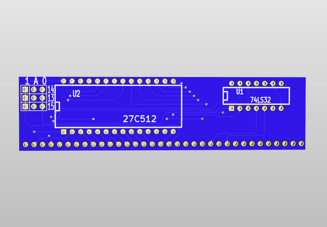
Address lines A13, A14 & A15 on the Z80 need to all be low for the Chip Enable to be triggered, which places it in the 0x000 – 0x1FFF address space. The RD and MREQ need to be low to trigger the Output Enable.
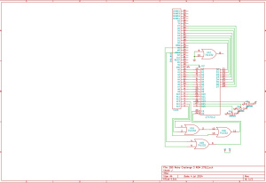
Click the image below for schematics in PDF format
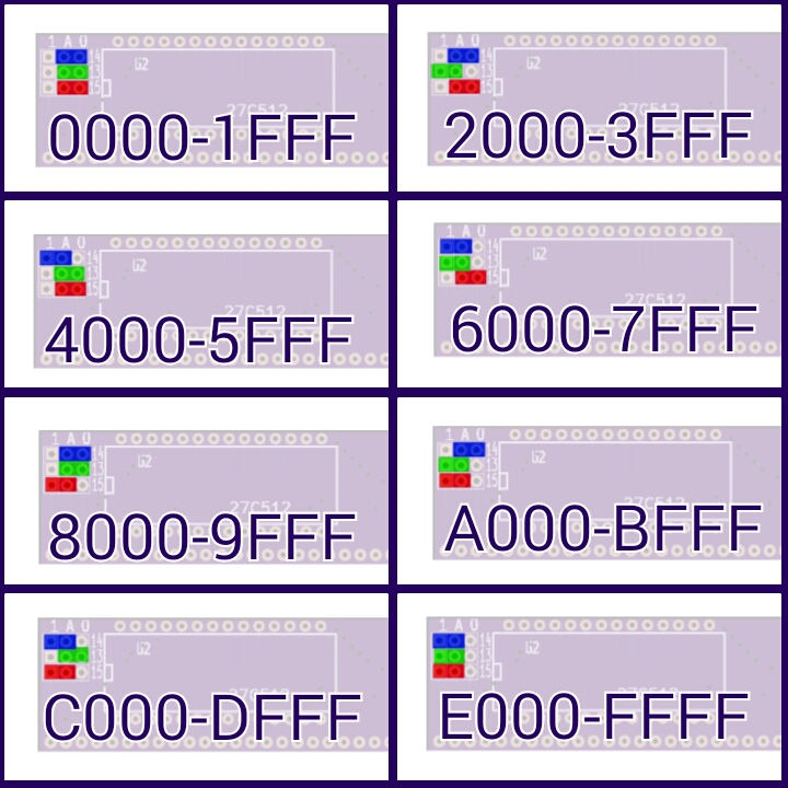
A 64K 27C512 is divided in to 8 x 8K (0x2000) with 3 jumpers to bring A13, A14 & A15 either high or low as per the illustration below. Note that all 3 jumpers must be used as leaving any of those address lines could give unpredictable results.
Although this was designed for a 27C512 EPROM, I have tested it with 27E512 (electrically erasable version) and it’s fine. It should also work with AT27C512R (non-erasable version) or with minimal modification the 27C256 (32K) and 27C128 (16k) chips too.
Buy one here
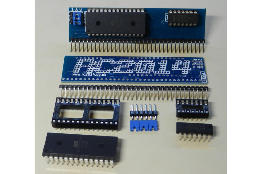
Bill of Materials
- 32 pin R/A header
- 28 pin wide DIL socket
- 14 pin narrow DIL socket
- 27C512 EPROM or similar
- 74LS32
- 3 x 3-pin header
- 3 x jumper