Having finished the first section of the Zero to ASIC course, I think it’s fair to say that I know a lot more about MOSFETs than I thought I ever would. MOSFETs are the building blocks of digital logic, so it is important to have a good grasp on why they are used, how they work, and how they are made.
There are several software packages and toolchains used for this course, and whilst they can all be downloaded and run locally on your own machine, I opted to download the virtual machine which has everything installed and configured. This lets me focus on the course itself rather than worry about installing the right version or having different settings. It also means I can swap between my laptop and desktop machine easily. Each section of the course has a GitHub repo to clone which includes examples and makefiles to do some of the heavy lifting.
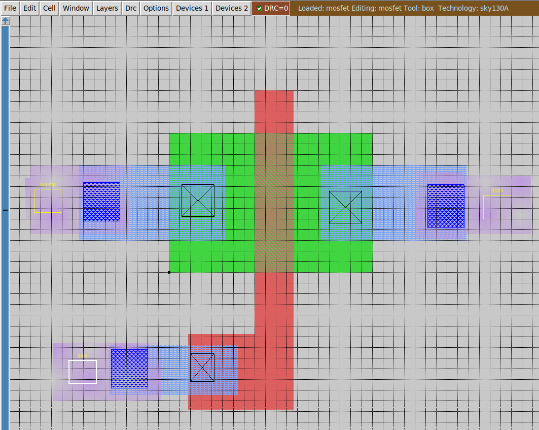
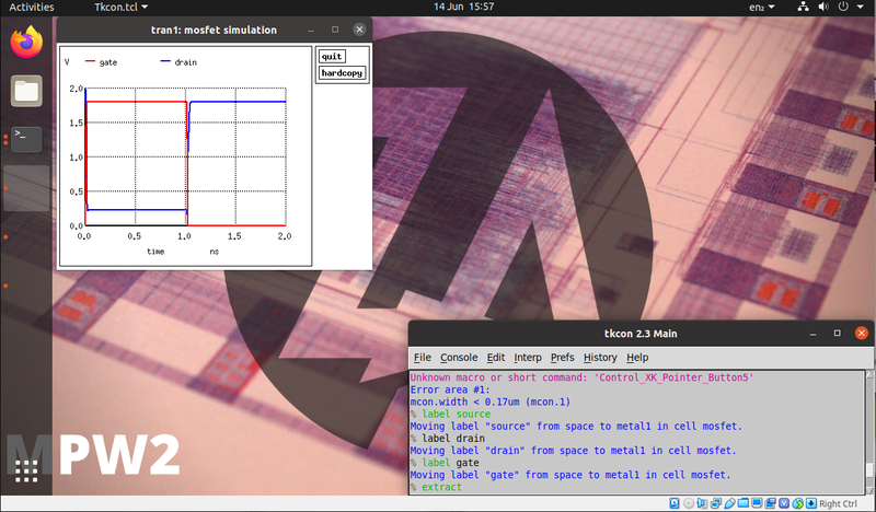
One of the pieces of software was a VLSI tool called Magic. Using this I was able to create a MOSFET by laying down layers of N diffusion, polysilicon, and metal interconnects and use the appropriate interconnects to join them all together. This was then exported so that it could be simulated in Spice to see how well it performed.
Although it would be possible to design my entire silicon project by drawing every single MOSFET by hand, luckily that isn’t necessary.
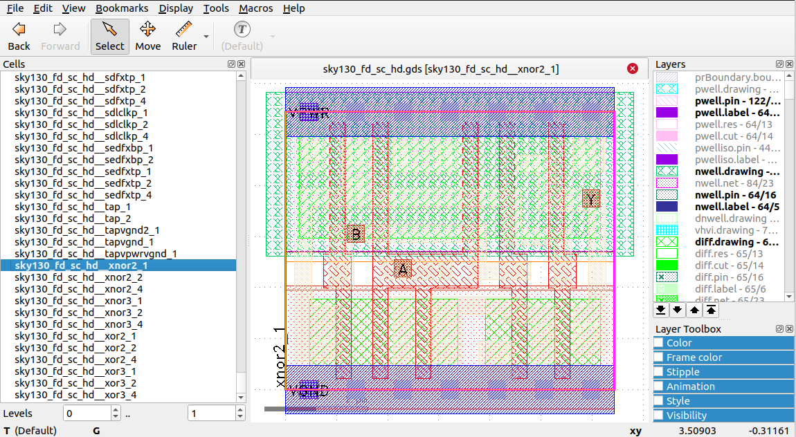
KLayout has a library of hundreds of different standard cells which can be used. This includes all the basic logic functions you’d expect as well as buffers, flipflops and other parts which I haven’t got a clue what they do!
I focused on a 2 input XOR gate. Again, though the use of Makefile scripts, I could export this part and run it through Spice to assess its performance.
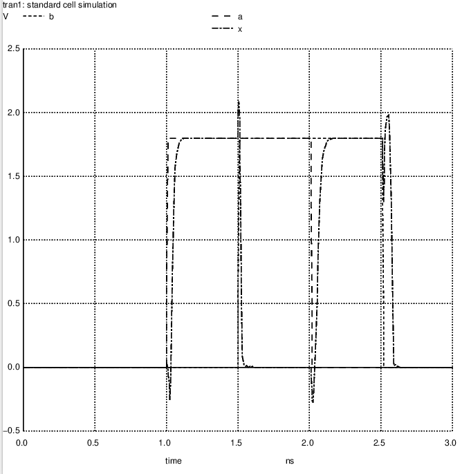
The parameters in the Spice configuration generates an offset pulse on the A and B inputs and plots a graph of the inputs and outputs based against time. Being an XOR gate, it is hardly surprising that the output is high when either A or B is high, but low when they are both high or both low. What was surprising, however, was the detail in the output, including the under/overshoot and the propagation delay. Whilst this might seem trivial on a simple gate like this, chaining hundreds of them together on the same piece of silicon you can see how that all adds up.
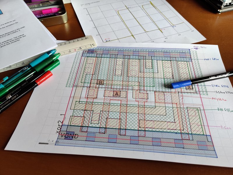
This is where I started to go down a rabbit hole. An XOR gate is, comparatively speaking, a simple device, only made up of a few MOSFETs and interconnects. I knew what a MOSFET looked like, so I decided to reverse engineer this so I could produce a schematic of it, and build it out of through hole components on a breadboard. For size comparison, this square of silicon is 0.0032mm on each side. Each leg on the through hole MOSFETs I have are approx 0.3mm wide.
Sadly, reverse engineering this proved to be a step too far for me. Whilst I could identify several MOSFETs with 100% certainty, things were not lining up with any of the XOR circuit diagrams I had already found. This is, however, well beyond the scope of this course though, and not something which should be necessary to end up with my own custom chip. It is something which I would like to come back to at a later date though, as I can see skills here being useful for other projects.