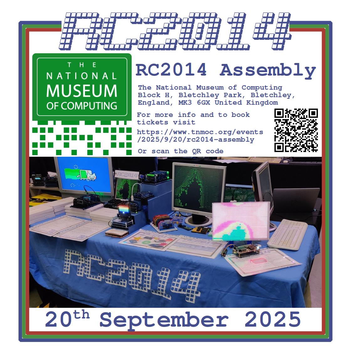
Last Year The National Museum Of Computing hosted the innaugural RC2014 Assembly v1.0. The first all-day event showcasing the RC2014 and similar modern retro computer kits was absolutely fantastic and I heard nothing but good feedback from other attendees, exhibitors and TNMOC staff. So we decided to do it all over again this year for the RC2014 Assembly v2.0 on 26th September 2026.
There will be demonstrations of various hardware and software, lightning talks as well as related kits available from various vendors. Meet and chat with other RC2014 users as well as some of those that have helped make the RC2014 what it is today.
If a day of seeing/talking/hearing about RC2014 isn’t enough, the ticket also covers access to the TNMOC itself which houses the world’s largest collection of functional historic computers and World War II machines, including Enigma, Lorenz, the working Turing-Welchman Bombe, the rebuilt Colossus (the world’s first electronic computer), and the WITCH (the world’s oldest working digital computer)
Tickets for the day can be booked on Eventbrite here
There are separate tickets for Exhibitors, Traders and General Attendance. The Exhibitor and Trader tickets include a table with power, free tea & coffee, and the option to set up late on Friday afternoon (with a possible pub trip on Friday night!) and an awesome RC2014 themed name badge :-)
Feel free to get in touch if you want to discuss your exhibit or anything else about the event.
This September The National Museum Of Computing will be hosting the RC2014 Assembly. The first all-day event showcasing the RC2014 and similar modern retro computer kits.
There will be demonstrations of various hardware and software, lightning talks as well as related kits available from various vendors. Meet and chat with other RC2014 users as well as some of those that have helped make the RC2014 what it is today.
If a day of seeing/talking/hearing about RC2014 isn’t enough, the ticket also covers access to the TNMOC itself which houses the world’s largest collection of functional historic computers and World War II machines, including Enigma, Lorenz, the working Turing-Welchman Bombe, the rebuilt Colossus (the world’s first electronic computer), and the WITCH (the world’s oldest working digital computer)
Tickets for the day can be booked on Eventbrite here
There are separate tickets for Exhibitors, Traders and General Attendance. The Exhibitor and Trader tickets include a table with power, free tea & coffee, and the option to set up late on Friday afternoon (with a possible pub trip on Friday night!) and an awesome RC2014 themed name badge :-)
Feel free to get in touch if you want to discuss your exhibit or anything else about the event.
Like many small businesses, RC2014 started as a personal hobby project. When there was an interest in the PCBs it was easy enough to sell those out of a spare bedroom. As things started to take off in 2016 I set up a limited company, RFC2795 Ltd, to manage the financial side of things. Gradually RC2014 started to take over more of the house for stocking kits and components, building prototypes, and packing/shipping kits.
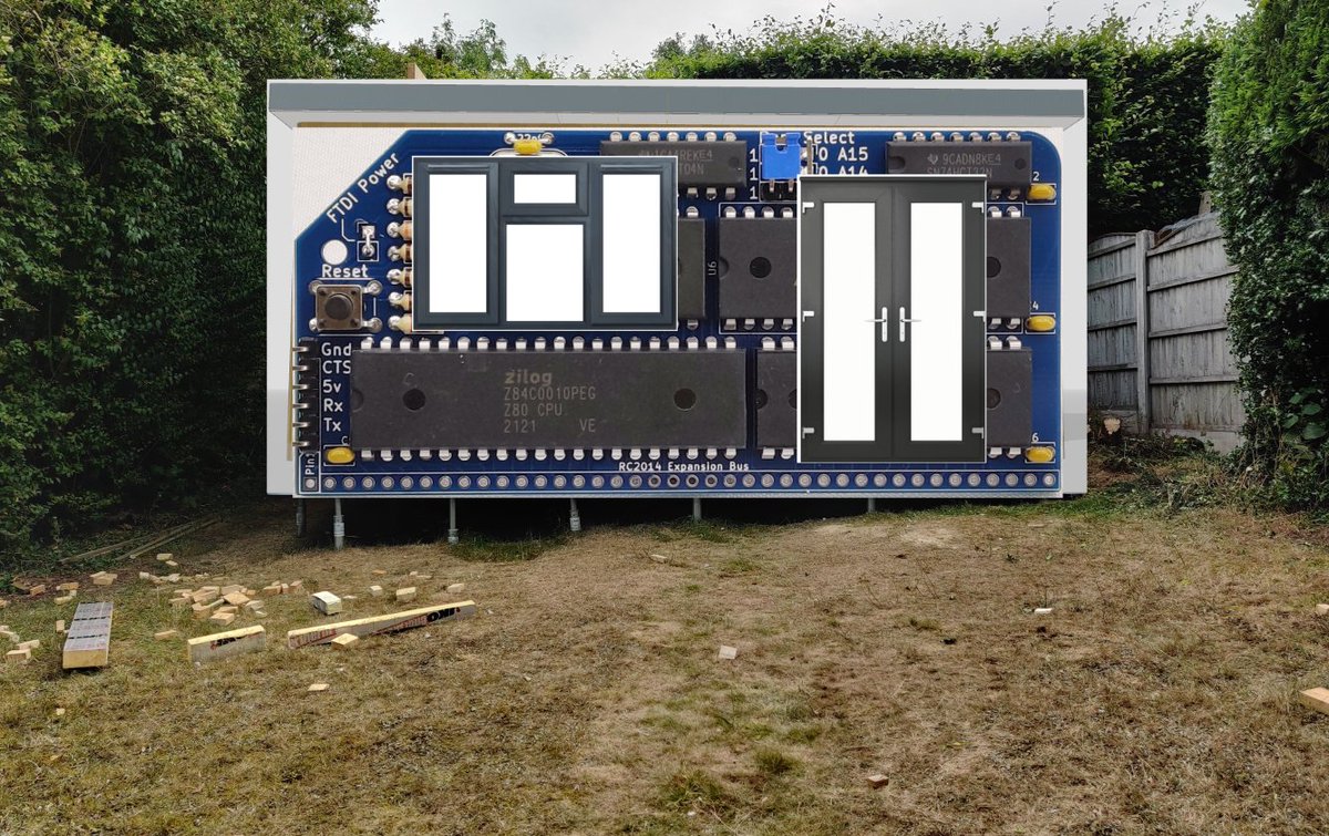
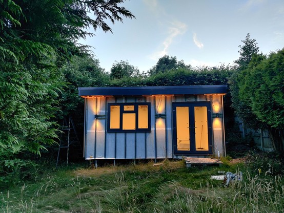
With space in the house getting more and more limited I looked in to the next step. Maybe renting an office? Rent a workshop? Move house? Buy a building for RC2014? In the end I settled on building a dedicated garden office. This allows me the home/work separation needed, whilst having minimal travel times. According to YouTube, it is something I should be able to build myself too, thus keeping costs to a minimum.
The design was a simple timber frame with flat pitched roof, large door, large window and probably clad with shiplap. The most important design aspect, however, was insulation. Lots of it. This needs to stay cool in the summer and be cheap to heat in the winter.
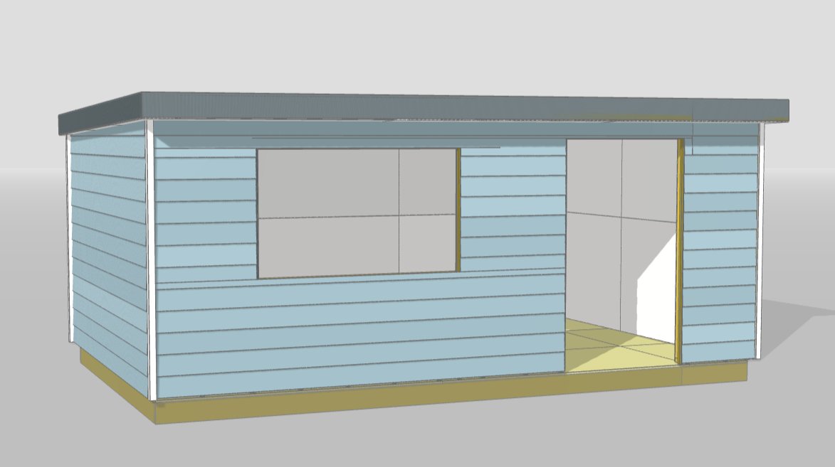
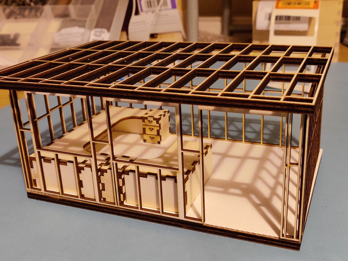
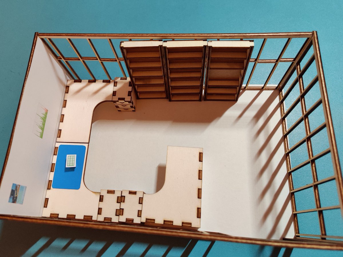
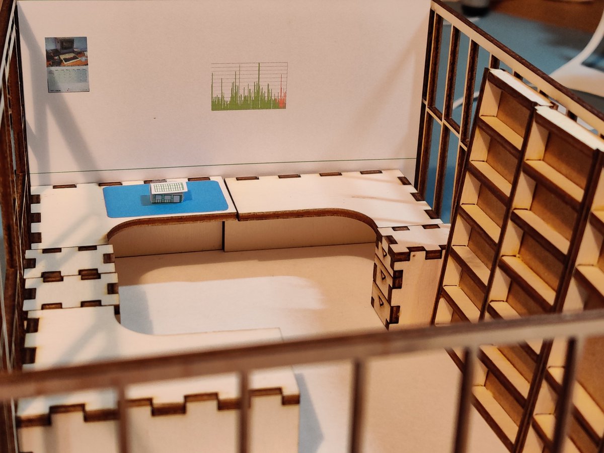
The bedroom that most of the RC2014 work is done in is 3.5m x 3.5. If the garden office was built 3.3m x 5.4m then it would be substantially larger, whilst being below the limit that would need planning application. To get a feel for the space, and see how things would work I laser cut a scale model and added scale furniture in it. Putting a scale model of the office on the desk in the scale model may have been a touch too much though!
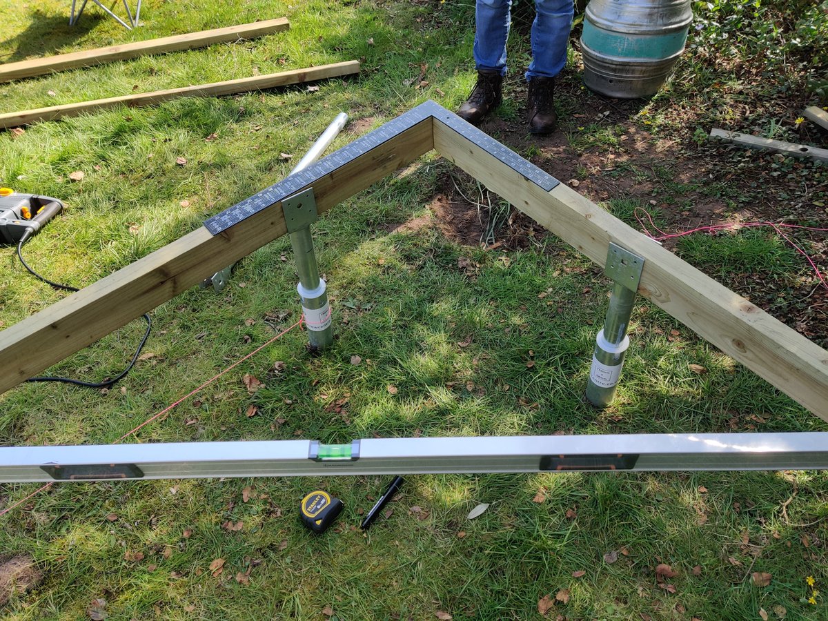
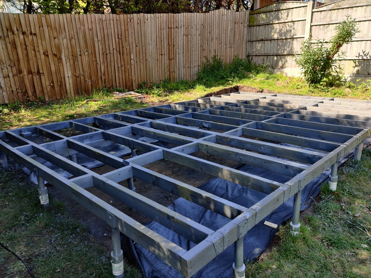
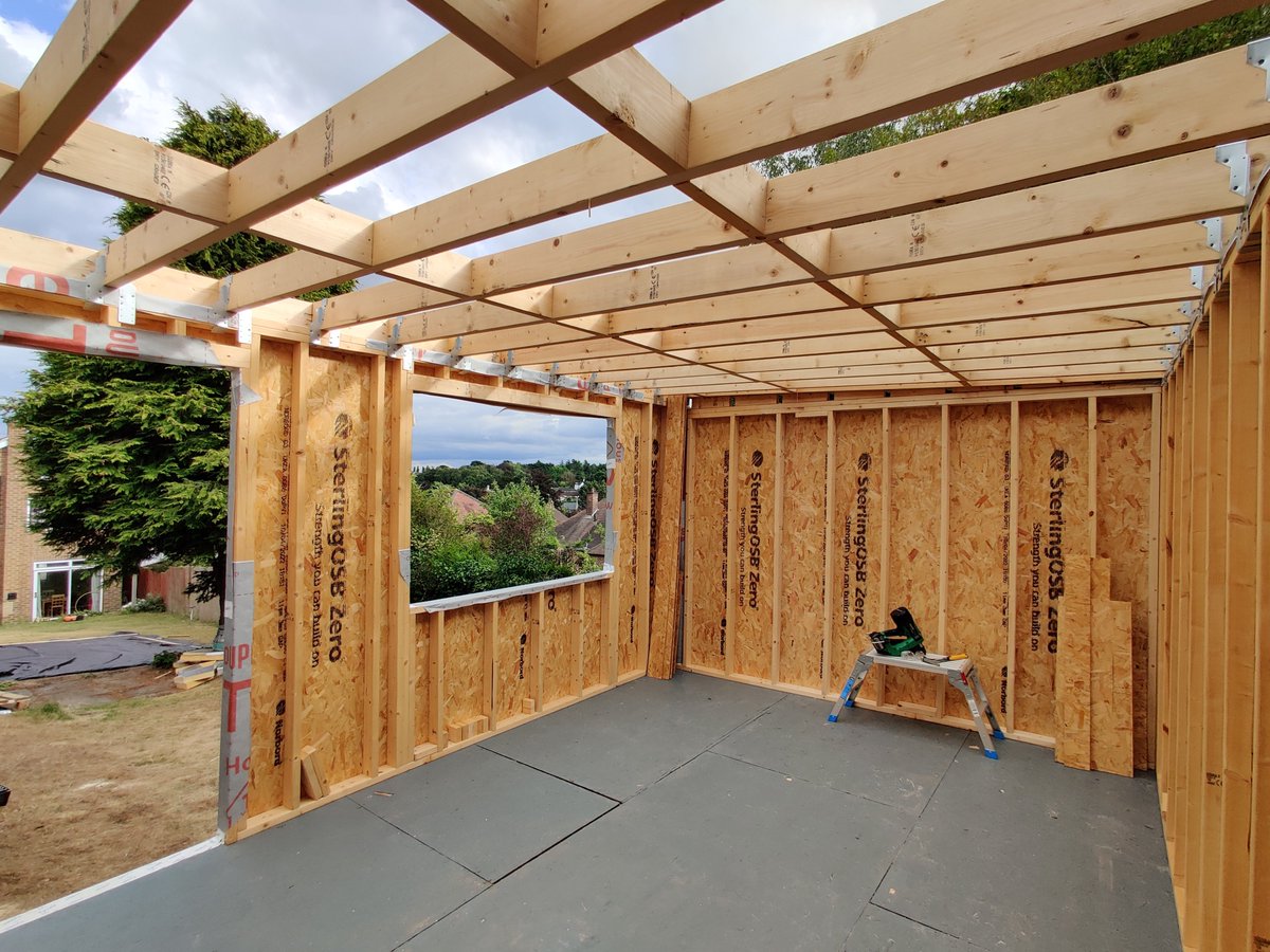
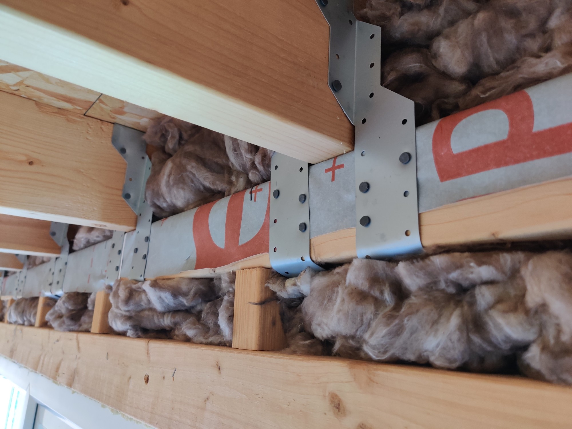
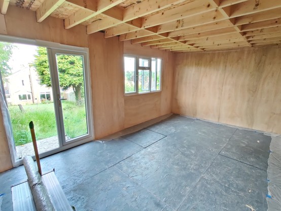
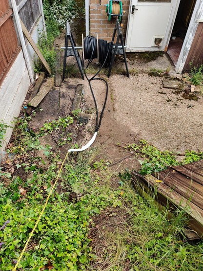
Work started in March 2022. Whilst I am lucky enough to have a garden with enough space for a garden office of this size, the garden is built on a hill which mostly slopes up from the house but also slopes right to left. This meant that in one corner the office would be over 0.5m above ground level, whilst in the opposite corner it would be about 0.4m below ground level. The subterranean corner was a lot of work to dig out, but worked in my favor because the limit on height for being exempt from building regulations is take from the adjacent ground level – thus giving me extra head height for a higher ceiling and more roof insulation. The timber frame was supported on ground screws which could be leveled out perfectly.
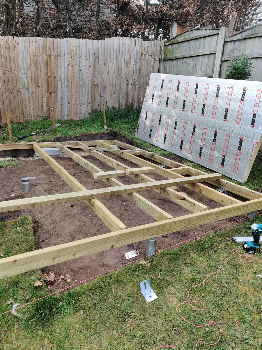
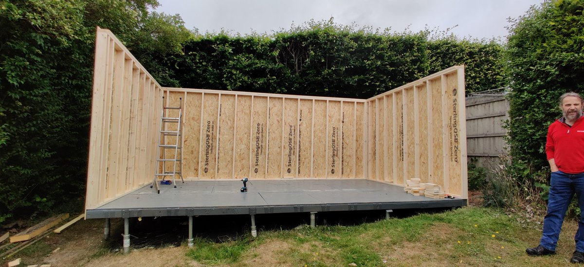
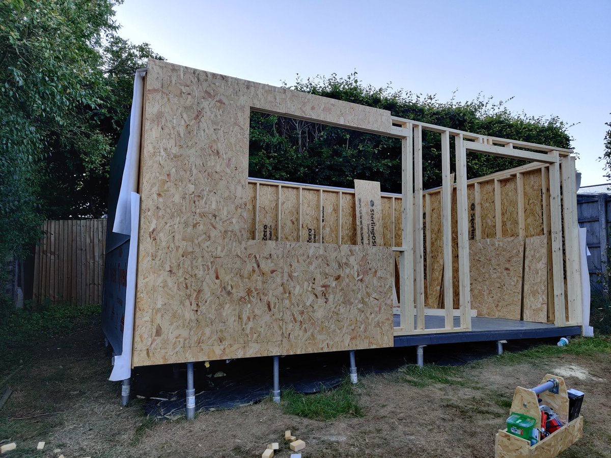
Over the very hot summer of 2022 the floor was installed and the walls erected. The elevation from road level meant great views, but carrying several tonnes of wood up to such a height was no small task. Whilst I carried out 99% of the work myself, the help of Shiela Dixon and Derek Woodruff was really appreciated.
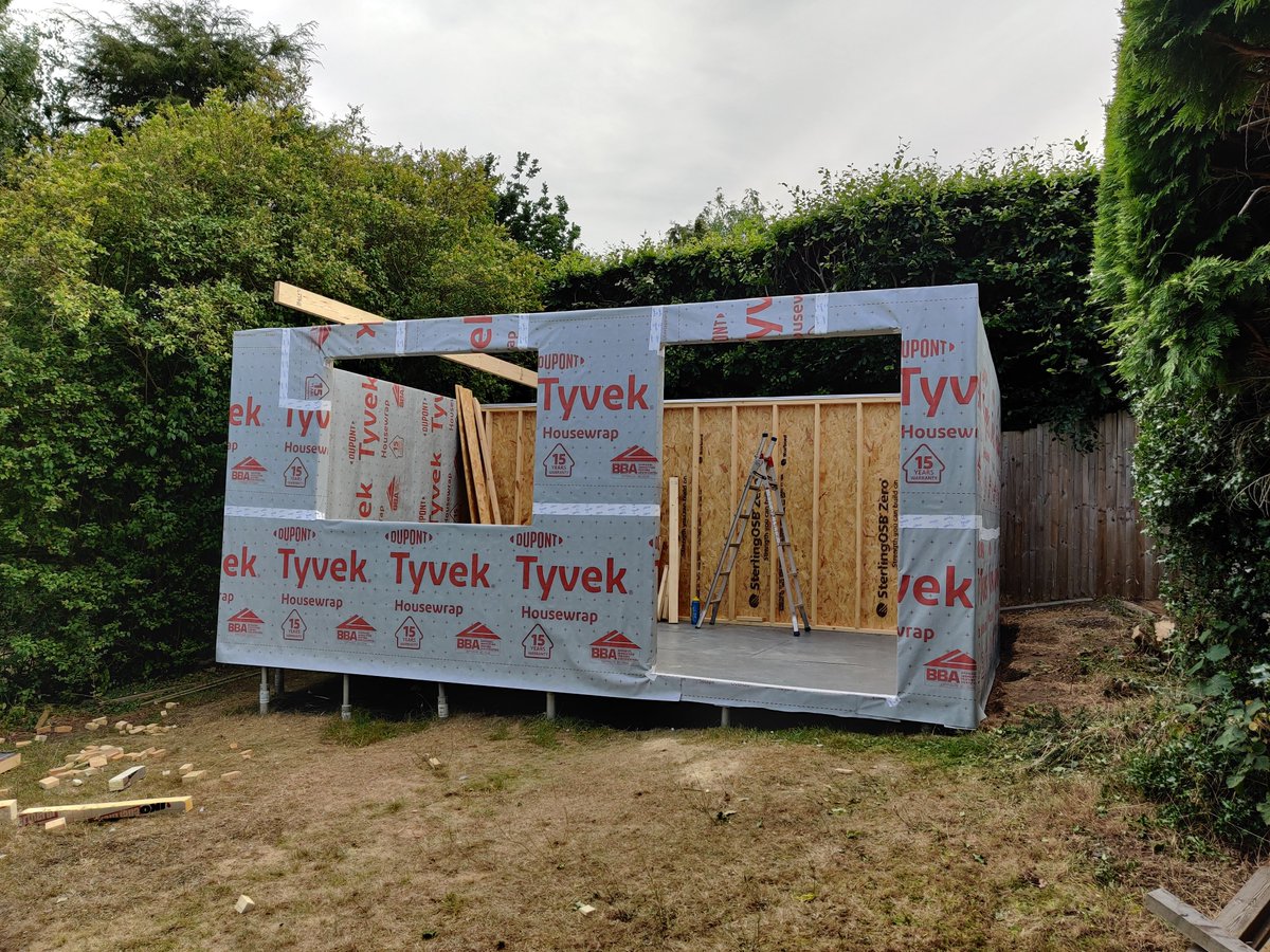
The goal for 2022 was to get to the stage of having a weatherproof box before winter. Thankfully this was achieved by the start of September.
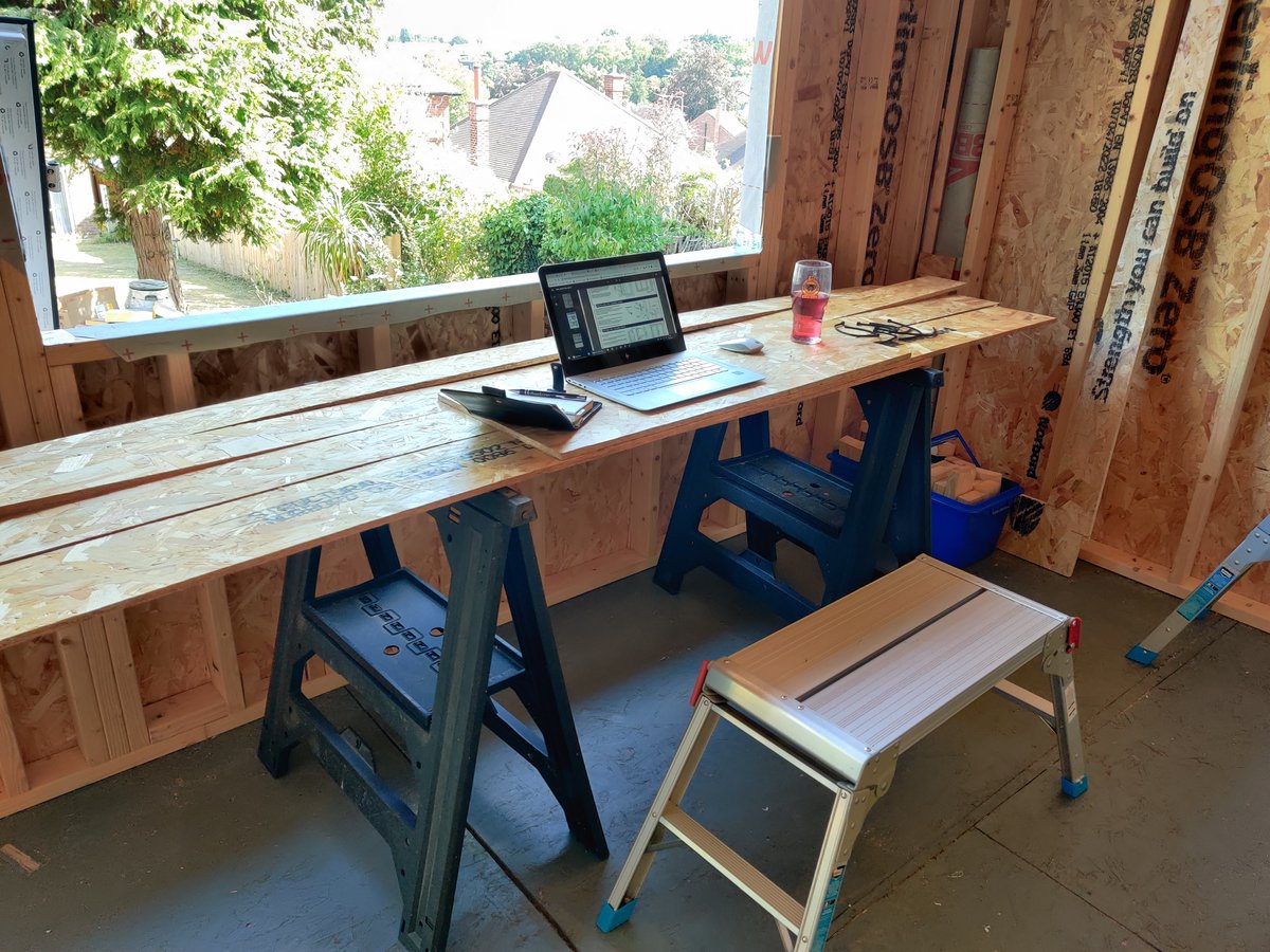
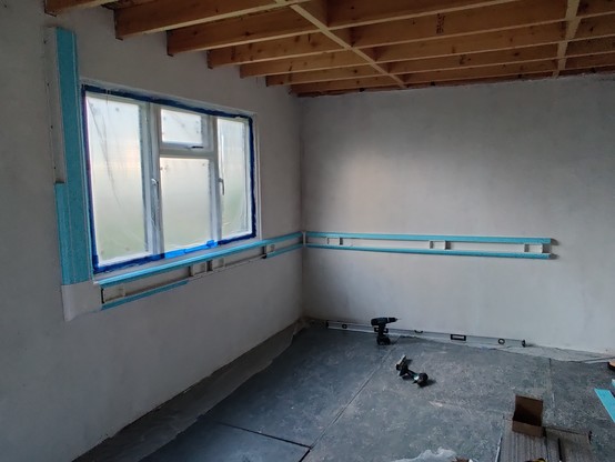
Not a lot of progress was made the following summer due mostly to a lack of time. 2024 however, saw a LOT of insulation going in before the walls were clad and painted internally.
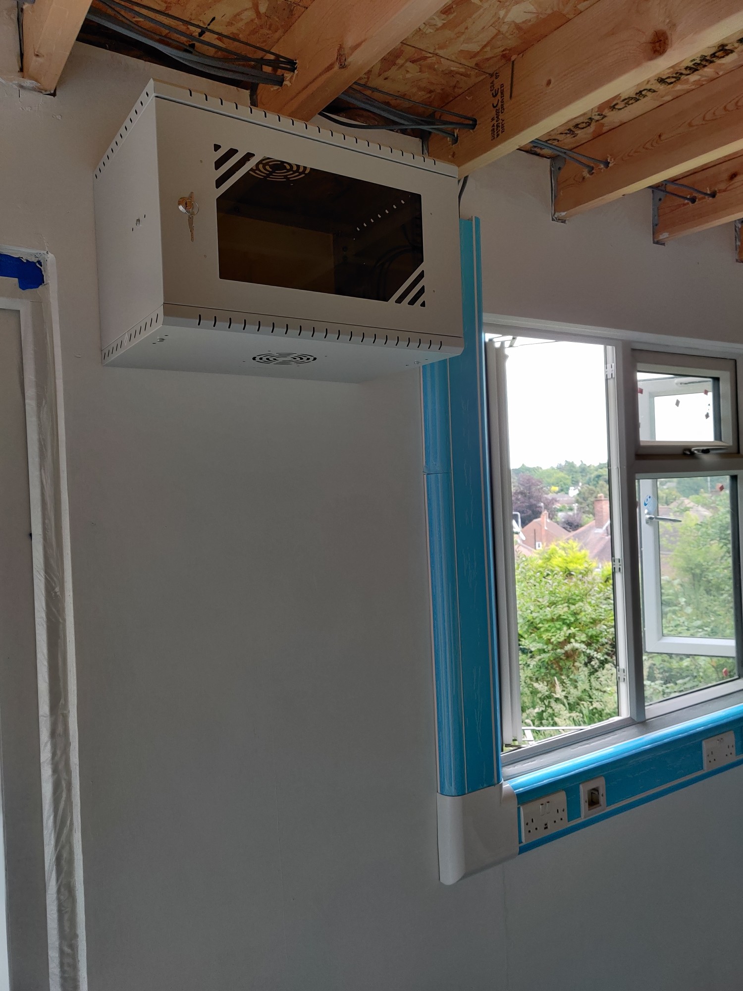
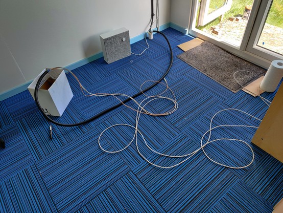
Inside the office I could run trunking and get things ready for the electrician to do his stuff. Whilst I probably could wire up the electrics safely myself, there are some jobs that I get a lot of peace of mind by paying a professional to do.
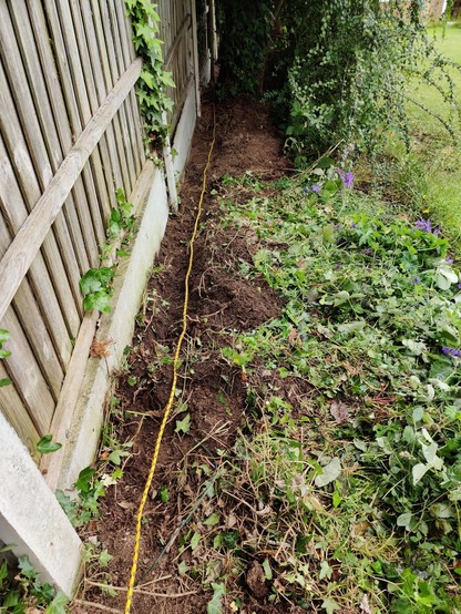
I ran the armored cable from the house to the office though, and that was much harder work than anticipated. Conduit for fiber and copper network cables was installed at the same time, but that wouldn’t be pulled through until the spring of 2025. Having power to the office was fantastic!
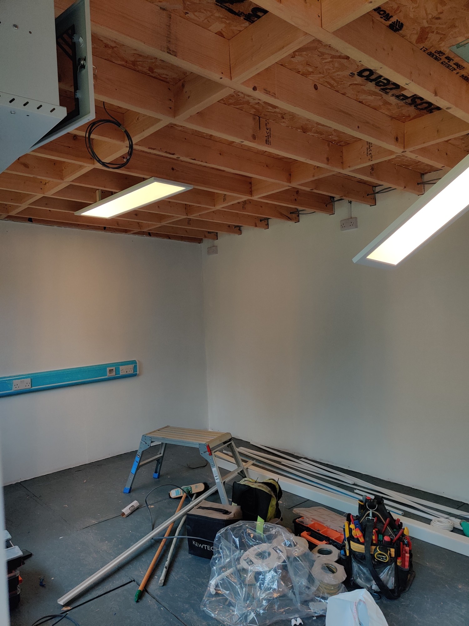
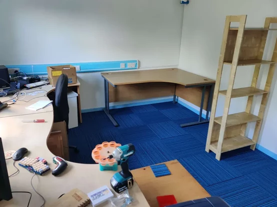
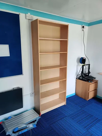
Now it was just the “easy” stuff like carpet, furniture, and moving in.
To make moving in as stress free as possible, z80kits was closed for a week at the start of June. Whilst I had been testing out the office with a few specific tasks, for the bulk of jobs it all needs to move in in one go. So everything related to RC2014 was moved from the spare bedroom to RC2014 Towers and allocated its new home in time to ship orders again on June 9th.
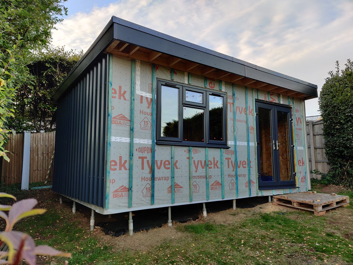
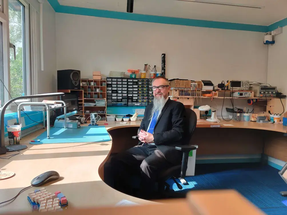
And there we are! Day 1 in RC2014 Towers and it is looking the neatest that it will ever look! There is 50% more surfaces to work on and 60% more storage too. This seems like overkill right now, although I know it won’t be long before I look back and wonder where all the space has gone!
When I started this build I was still on Twitter and I tweeted updates. The archive of those tweets is available here https://rc2014.co.uk/twitterbackup/rc2014towers/ (Select Browse and Oldest First for the chronological view). These days I use Mastodon, and you can follow the #RC2014Towers hashtag for updates https://mastodon.me.uk/tags/RC2014Towers
Following on from the failure to get the Portfolio talking directly to the RC2014, I decided to turn my attention to the Cambridge Z88. I already have a custom RS232 to TTL serial adapter for that, and the RC2014 is all set up ready for the Portfolio at 9600 baud, so this should be straightforward…
Well, would you believe it, it was a success! The Z88 is a fantastic machine, with some good built in programs. One of those is a terminal emulator, so it really was just a case of plugging the RS232 adapter in to the RC2014, with Port B set as the primary port set at 9600 baud.
To test it properly, I typed in the test program for the LCD module https://rc2014.co.uk/modules/lcd-driver-module/ (The initial test failed, but after I plugged the LCD in correctly, everything worked fine).
Buoyed on by the success there, I decided to turn my attention back to the Portfolio. Knowing that the Z88 RS232 to TTL serial adapter worked meant I didn’t have to burn my fingers again! The only issue was that the Z88 had an almost but not quite standard pinout on the DB9
I blogged about the Z88 RS232 to TTL Serial adapter back in 2013 https://sowen.com/466/z88-to-ftdi-lead-via-max3232/ The important takeaway from this is that Gnd is on Pin7 on the Z88, although it is Pin5 on the Portfolio. It is also worth noting that Pin1 and Pin9 both carry 5v, and whilst these aren’t used in my adapter, they could break other things they are plugged in to. Pin2 and Pin3 are Tx adn Rx respectively on both the Z88 and Portfolio.
Time for a Frankenconnector to adapt them!
The other bit of unfinished business on the Portfolio was putting some terminal software on there. A copy of xterm2, as supplied on the Portfolio utility card was easy enough to find. In the past I had transferred programs to the Portfolio via the parallel adapter, however, I had recently bought an APF-01 memory card from https://apfram.com/ Whilst I had to use some propriety software on a Windows machine to copy the files on to it, it worked really well.
With everything connected up and Xterm2 started, the Portfolio and RC2014 were talking!
Again, I typed the LCD test program and sent a message to be displayed from the Portfolio to the RC2014
Although, of course, it was only as I type this blog post that I notice the Off-By-Ten error in that message! Ooops!
So, that is the Z88 and the Portfolio both ticked off of the list of computers to talk to the RC2014. Whilst the Portfolio wasn’t a complete failure before, I am really glad I revisited this and got a more satisfying result. And it has reminded me just how good both of those two machines are. I really should use them more.
2024 marks the 10 year anniversary since I entered the Retro Challenge in… hmmm… let me see now… that’ll be… 2014! Yes, I remember it well, because Retro Challenge 2014 had a catchy hashtag on Twitter, something like #RC2014.
Well, the good folks behind Retro Challenge approached me and asked if I would consider donating a prize for this years event. There were no prizes back in my day, it was all about likes and subs, and inadvertently starting a new career back then. But, hey, I understand that people like prizes, so I said yes. I said I would like to offer an RC2014 Classic II kit to the winner of the RC2014 category
After thinking about it for a little while, I figured I could come up with something a little bit more special. But before I reveal what that is, and before you skip to the bottom of this post for a sneak peek, I wonder if I should explain what Retro Challenge is. Well, it is a challenge revolving retro computers. The challenge is self-set, and you can do pretty much whatever interests you if it involves a retro computer, and you blog about it to share your knowledge and inspire others. Maybe you want to right software for your old Dragon 32, or get that VIC20 cleaned up, recapped and retrobrited, or scan in the original PDP manuals and upload them to the Internet Archive.
Back in 2013 I had built a Z80 computer on a breadboard that ran BASIC. The challenge I set myself for Retro Challenge 2014 was to make my name appear in lights. More specifically I was going to write Z80 code to do it, using a Z80 computer which I also had to design. You can read more about it here https://rc2014.co.uk/653/retro-challenge-2014/
Part of the challenge was to get the PCBs designed and manufactured. I used OSHPark which meant I had 3 of each board. Luckily the designs worked and no serious modifications were needed (although a hammer was required to fit the header pins). You can read about the boards arriving here https://rc2014.co.uk/791/retro-challenge-pcbs-arrived-and-built/
Of the three sets of PCBs I had made, one set was used to build my original RC2014. Obviously. Another set was traded with John Fletcher for an original unpopulated Jupiter Ace PCB (See https://sowen.com/995/ace-adventures-on-jupiter/), and the feedback from that made me wonder if I should get some more made in case anybody else wanted to build their own RC2014.
So, what about the third set? It could be yours!
That’s right. In addition to the RC2014 Classic II kit, I will be giving away the final set of the original RC2014 PCBs to the lucky winner. Well, the original 32k RAM, Pageable ROM, Serial I/O and clock/reset module. The CPU module is a later one which the PCB manufacturer screwed up and didn’t put the silkscreen on the back! And I will throw in an original Digital I/O PCB too. As well as some stripboard.
Everything needed to complete the build is part of the Classic II kit. So when you receive your prize, you will need to decide if you want to build it as a Classic II, or go old school and make the most authentic RC2014 there is.
Not sure if I should put some legal disclaimer here or whatever. The winner will be chosen by the Retro Challenge organisers. I will post out the Classic II kit along with the original RC2014 PCBs mentioned above to the winner within a month of the winner being announced. This includes free international shipping if you are outside of the UK. No cash alternative is offered. Neither myself or the organisers of Retro Challenge can be held liable if you end up starting a new career based on your competition entry.
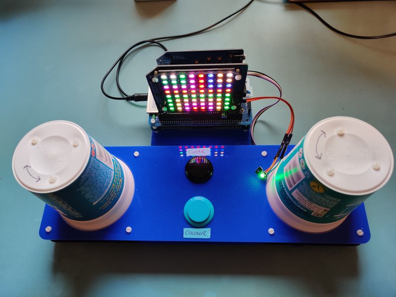
In July 2024 I was exhibiting at Liverpool Makefest again. This is a fantastic family friendly makers event that is open to the public for free. It has always been a great place to show off the various RC2014 kits as well as have something interactive that can keep people entertained.
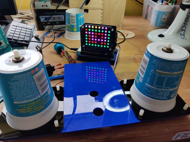
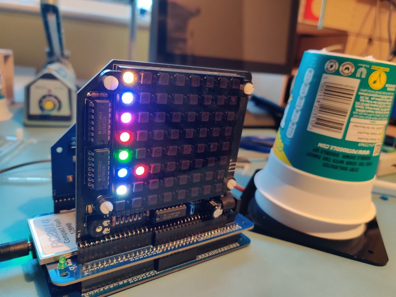
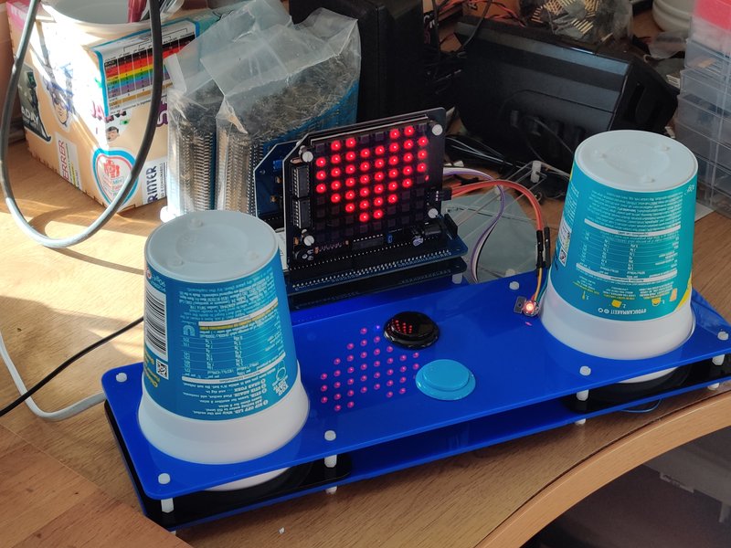
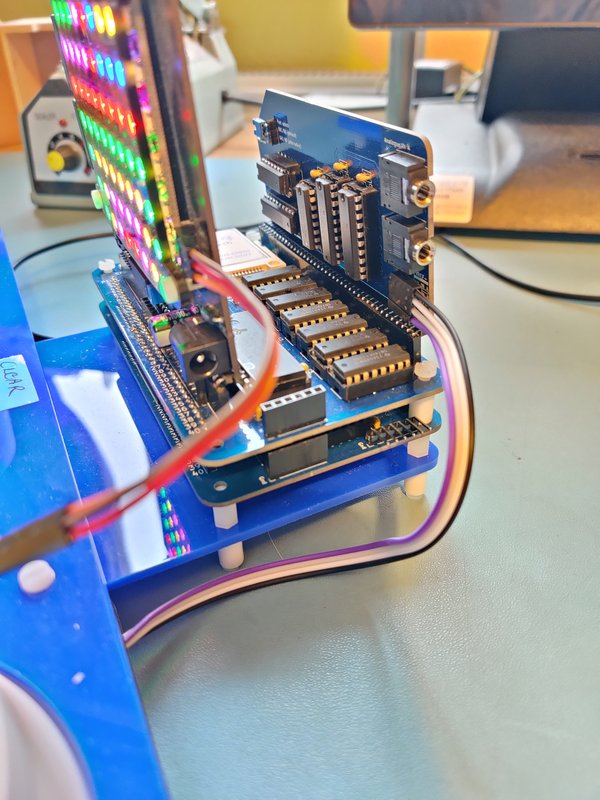
Normally I have a machine set up running Snake, but this year I was about to launch the Dual Paddle Analogue Module, so I wondered about making something with that. The idea of an Etch-a-sketch came up, and coupled with a NeoPixel Matrix Module I figured this would be a nice self contained demo unit.
I could handle the electronics and the physical build, but I reached out to Shiela at Peacock Media to see if she could help on the software side. As both the Dual Paddle Analogue Module and the NeoPixel Matrix Module were Shielas design she jumped at the idea. it was only 5 days before the event though, so we needed to move quick.
There were some important design considerations. Firstly, it had to be robust. One thing about the audience at Liverpool Makefest is there are quite a few kids and they are not always gentle with the exhibits. It also needs to be intuitive. If people need to read instructions, or things don’t give a satisfying output in the first few seconds they you have lost them. On top of that, it should really be self contained to the point where there is no need for a monitor or keyboard, and it just runs as soon as power is applied.
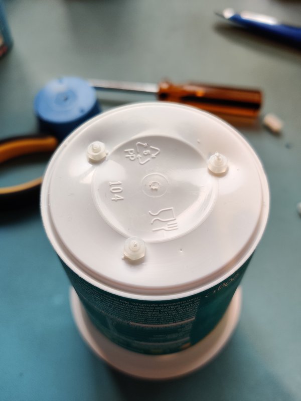
The first thing I needed to work out was the control mechanism. Two potentiometers, obviously, for X and Y, but how are they going to me mounted. I ran through some gamepad type prototypes but things weren’t quite feeling right. Then I noticed a couple of Pot Noodle pots sitting on my desk. These tapered plastic pots are great for pencil pots or other storage, and they stack really nicely. Two stacked together actually turn really nicely and feel good. But could a Pot Noodle pot house a pot? The Pot Noodle was launched at the same time as the Z80, so it seems like destiny, right?
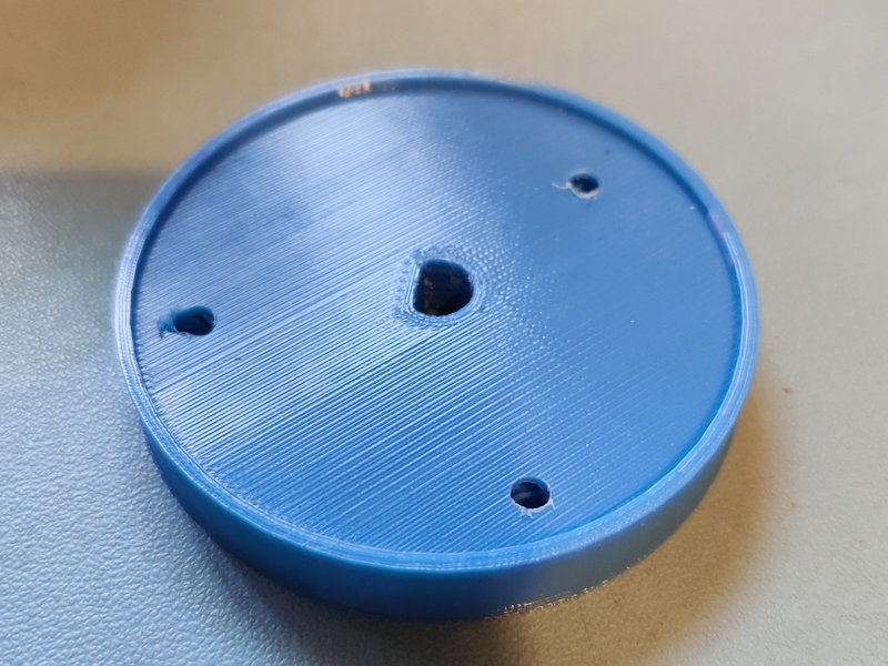
Off to the laser cutter to knock up a prototype. This consisted of a flat square plate with 3.5mm holes in the corners, and another matching plate that had a 100mm hole. This hole was slightly smaller than the brim of the pot, so when screwed down it holds the pot really really tightly to the base. With another pot on top it rotates really well. Putting 10mm standoffs and another pate with 100mm hole in it still allows it to rotate and it prevents the top pot from coming off.
fixing a 10k linear pot to the lower pot was easy enough. I used these lovely vintage RS pots that have a D-shaft
However, fixing the top pot to the shaft was a challenge. Making a D-hole in the top didn’t sound robust, so I decided to 3D print a couple of parameterised knobs in OpenSCAD. I could then glue these inside the top of top pot.
Dear reader, let me share one thing I now know about gluing PP (Polypropylene) plastic that the pots are made of PLA (polylactide) the 3D print it made of – you cannot! There isn’t a glue or solvent that will work. Trust me, I tried many many things.
However, mechanical fasteners (M3 nuts and bolts) do work! The image above shows some holes drilled in the 3D part. Similar holes were drilled in the pots and they were bolted together. Rugged, child-proof and even repairable if needed!
This could now sit on the D-shaft of the pot, and kept from being removed by the top plate.
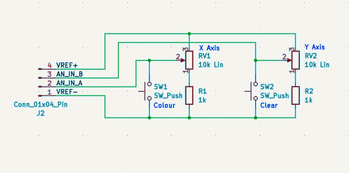
Next the question about additional controls. Whilst the original Etch-a-sketch was monochrome, the NeoPixel display didn’t have this limitation. There are a few ways to add a digital button to an RC2014, but when there is already an analogue module plugged in, it would be nice to use that.
To achieve two buttons of input, a 1k resistor was added to the negative side of the pot and a switch on the wiper going to ground. In normal use the 8 bit value from the variable resistor will only go down as low as 23, and as high as 255. When the switch is pushed the value is 0. So the software only needs to map approximately 25-255 to the 8×8 display, and anything less than 10 can be treated as a button press. With two pots, this allows 2 buttons, one for to cycle the colour, the other to clear the screen.
Note that it is tempting to put a 1k resistor and another switch going to the 5v line. This will give an extra two buttons, which would be great. However, if both buttons are pushed at the same time it will be shorting 5v and ground. This is a Bad Thing™ and certainly not something you want on a public facing exhibit. Even with a “do not push both buttons at the same time” sign!
A couple of arcade buttons worked great for this, although a label was put on as an afterthought as they weren’t quite as intuitive as hoped.
Shielas software worked great! Burning this on to ROM meant that it just ran on startup without any faffing at all. And with a t-shaped frame that housed the two pots, the buttons, and an RC2014 Mini with NeoPixel Module as well as the Dual Paddle Analogue Module it was a really nice self contained unit.
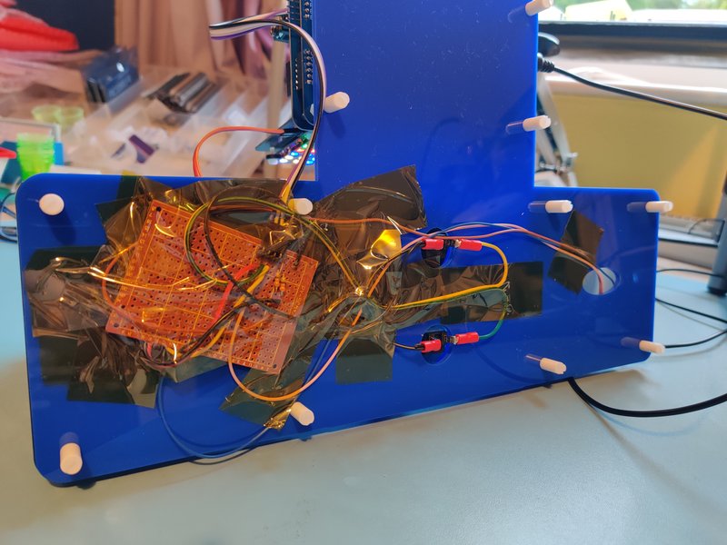
Things aren’t quite so neat underneath as the wiring for the pots and switches are all routed to a prototype board held together with Kapton tape. But nobody ever looks underneath, right?
How did it go? Great! As always, Liverpool Makefest was a great day out. The folks in Liverpool seemed to instinctively get it straight away. Some people spent a while creating their own Mona Lisa, and others tried teamwork with one person controlling the X axis and the other controlling the Y axis. Nothing broke down or needed restarting and it is all ready for the next event. If anything, the only failing was that it worked too well that nobody particularly asked how it was working, so I didn’t get to talk about the analogue module too much. But at least I got a blog post out of it :-)
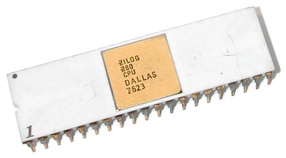
For those of you that haven’t heard, on 15th April 2024, Littlefuse, the parent company to Zilog, announced the End Of Life of the Z80 and associated peripherals https://www.mouser.com/PCN/Littelfuse_PCN_Z84C00.pdf and it is fair to say that this has sent shockwaves through the retro computing community. In the wider electronics community there has been shock too, although some of it was that the Z80 was still in production 48 years after it launched.
There have been a lot of hot takes on this news, some of which seem to jump to bizarre conclusions or unrealistic solutions. A few people have been in touch either privately or publicly asking me what is going to happen and what can be done about it. I don’t have the answers, although I do have my own hot takes.
What the announcement means
Firstly, reading the announcement properly, the Z80 has not ceased production yet. However, it is the last chance for suppliers to get their orders in. The likes of Digikey, Mouser, RS, Farnell etc have until June 14th to place their orders, then sometime over the following 24 weeks the final batch will be manufactured. I don’t know how many chips will be ordered, but I suspect it will be quite a lot, and hopefully enough to sustain the hobby for many years to come. Sadly, this seems to be in the hands of the buying departments of the aforementioned companies. I don’t have any contacts there, or any influence over them, but if anybody reading this does, please get in touch.
Also, the particular announcement linked to above lists the Z80 chips associated with this EOL, however, there are several other announcements that cover the Z180 as well as the peripheral chips like the SIO/2, PIO, CTC etc. This covers the 40 pin DIP variants we are all familiar with, as well as the LQFP-44 and PLCC-44 variants. Throughout this post I will refer to the Z80 as shorthand for the family of Z80, Z180, and support chips.
What the announcement does not cover is the eZ80, which is likely to continue to be manufactured for quite some time to come. Whilst the eZ80 is somewhat backwards compatible with the Z80 and Z180, it is by no means a drop-in replacement. Making changes to existing hardware and software to take this 100 pin LQFP package is non-trivial, but it isn’t out of the question.
Hobbyist Predictions
As a hobbyist with a love of the Z80, I find this news very sad, although it is not as devastating as some of the hot takes will make you believe. I think that new Z80 chips will be in stock with the retailers for several more years, although there will inevitably be a price rise as supply runs down. Even after then, the market in reclaimed chips, “new” stock from china, FPGA based clones, and other solutions will come up and keep computers and hobby projects going for many years. It will undoubtedly cost a few dollars more for each chip, and reclaimed chips will always be a bit of a gamble, but it is an affordable price for a great hobby.
Z80Kits Predictions
As a business owner of z80kits.com, a site that as the name suggests, is dedicated to the sale of kits based around the Z80, I find this news quite devastating. Over the past 8 years I have sold almost 5000 kits with a Z80 in them, plus a lot of extra modules that make use of the Z80. The EOL of the Z80 is signalling an EOL of z80kits. However, the timeline for this depends mainly on the buying departments of Digikey, Mouser, RS et al. which is an uncomfortable place to be in. And whilst a few dollars on the cost of a single chip might be affordable for a hobbyist, as a company that orders chips in quantities of 100 at a time, this is going to have some financial challenges too.
As mentioned above, there are alternatives. Reclaimed chips are not an option, as selling a kit has an implied assurance that the kit will work. Troubleshooting a users build when even the CPU is an unknown quantity is not something that me or the customer wants. The eZ80 or an FPGA will probably be the most likely contenders, although they will inevitably require a lot of R&D, and sadly lose a lot of the nice retro 40 pin DIP appeal that the Z80 has.
In the short term, however, I am not expecting things to change very rapidly. A decent supply of chips is always kept on hand, and that should last until the suppliers get their stock from the final production run. As long as the suppliers have made their predictions correctly, then things should just carry on as they have been. But if the suppliers decide that there isn’t enough profit in old components like this, then the outlook is much less rosy. We will have to see…
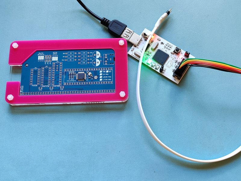
Sometimes an RC2014 has just one job. This one is to go Beep Whoop, Beep Beep Whoop, Beep Beep Beep Whoop! whenever a working Why Em-Ulator Sound Module PCB is put on the jig.
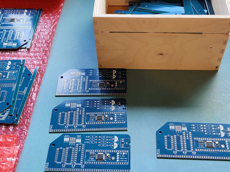
Before we get to that, though, lets go back to the start and consider the Why Em-Ulator Sound Module. This is supplied to RC2014 Towers with the surface mount components assembled and the PCBs panelised. The panelisation is needed so that they will go through the assembly process at the fab house. So the first thing to do is remove the rails and separate the pair of boards.
Removing the rails is made easy with a slot cut in to a wooden box. The rails are put in to the slot and a quick bend up and down detaches them from the main PCB. The discarded rails are then collected in the box. Breaking the two PCBs apart is also a simple process.
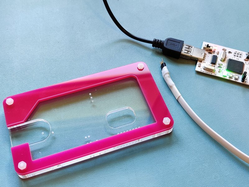
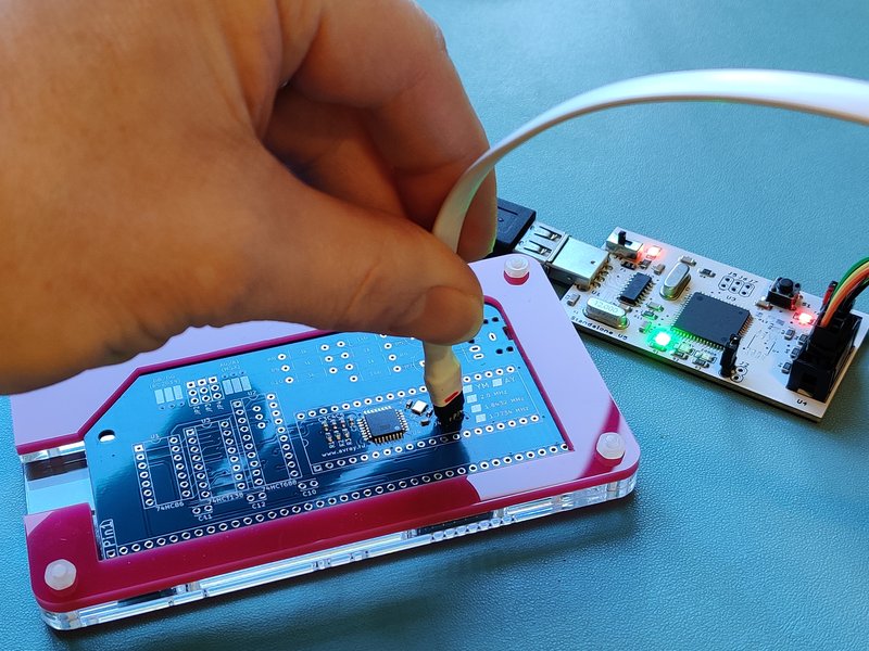
Next the micro controller needs to be programmed. The PCB has a TC2030 Tag Connect compatible programming header next to the micro controller. The programming cable has spring loaded pogo pins and some locating pins that protrude through the board. To accommodate this, a small jig (Jiglett) is used.
The programmer is a stand alone device which has the flash hex file, eprom hex file and fuse settings for the default Why Em-Ulator settings (YM2149 at 1.7734MHz). Other settings can be programmed manually from a laptop.
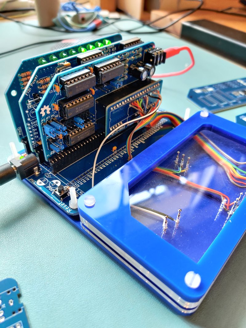
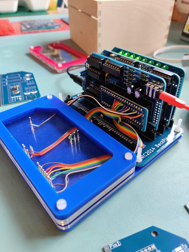
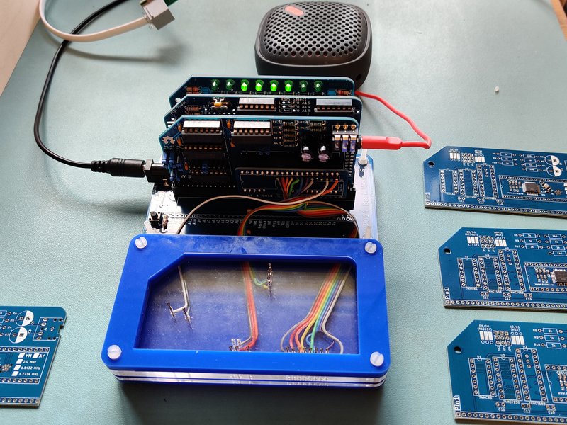
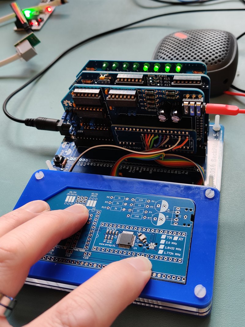
For peace of mind that the firmware has been programmed successfully, and that the assembly process was correct, it needs to be tested. This is where the Jig-Ulator comes in.
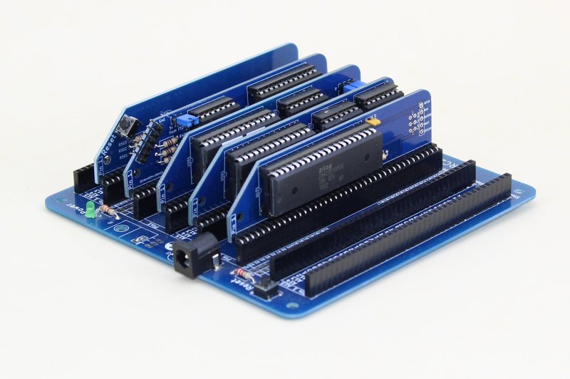
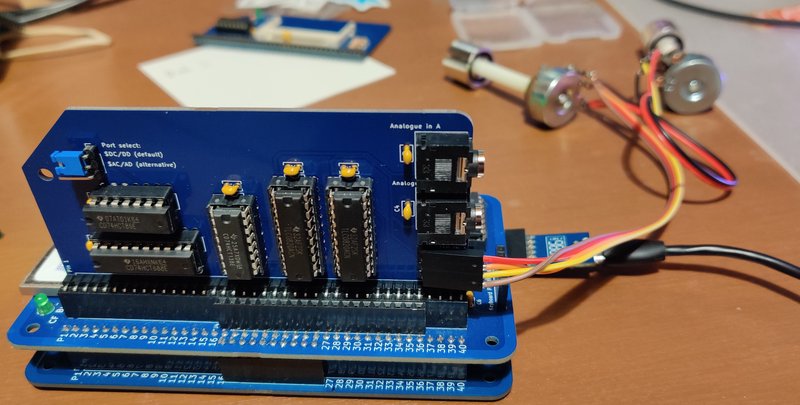
At the heart of the Jig-Ulator is an RC2014 Micro. This sits in a Backplane 5 with 3 sockets fitted. One of these sockets has a Digital I/O Module for visual feedback and the other has a Rev 5 YM2149 Sound Module with an AY-3-8910 to AY-3-8912 adapter. This adapter carries all the signals (Power, 8 data lines, Reset, BC1 and BDIR) that the Why Em-Ulator needs to operate, as well as the return path for the sound from Channel A, Channel B and Channel C. The sound module is plugged in to a speaker for audio feedback.
At the front of the Jig-Ulator is a bed of nails test jig made from laser cut Perspex and pogo pins. The Perspex holds the pogo pins in place, and the upper layers have an alignment cutout so that the module under test will line up perfectly with the pins. A little bit of pressure ensures that all signals make good contact.
The RC2014 Micro has some very simple test code in ROM that runs on startup and continues indefinitely. This code isn’t elegant. Nor is it particularly efficient. And it certainly isn’t an example of how to write good Z80 assembly code. However, it has one job, test the module, and it does that well.
All of this only takes up a couple hundred bytes of the 8k ROM. It can surely be optimised to take up less space. Alternatively, the calls can be unrolled to take up more space but without needing any RAM for the stack.
            .ORG    $0000
REG         EQU     $D8
DAT         EQU     $D0
START:
            NOP
            NOP
            DI       ; disable interrupts
            LD      hl,$9000
            LD      sp,hl ; set up stack
            NOP
;set mixer reg to enable channel A
            LD      a,7
            OUT     REG,a
            LD      a,62
            OUT     DAT,a
            LD      a,15
            OUT     0,a ; set DIO lights right

;set channel A to max volume
            LD      a,8
            OUT     REG,a
            LD      a,15
            OUT     DAT,a

;output 2 note to channel A
            LD      a,0
            OUT     REG,a
            LD      a,128 ;low note
            OUT     DAT,a
            CALL    delay
            LD      a,255 ;high note
            OUT     DAT,a
            CALL    delay

;decremental tone
            LD      a,0
            OUT     REG,a
            LD      b,255
            CALL    ALOOP

;set mixer reg to enable channel B
            LD      a,7
            OUT     REG,a
            LD      a,61
            OUT     DAT,a
            LD      a,$F0
            OUT     0,a ; set DIO lights left

;set channel B to max volume
            LD      a,9
            OUT     REG,a
            LD      a,15
            OUT     DAT,a

;output 4 note to channel B
            LD      a,2
            OUT     REG,a
            LD      a,255 ;low note
            OUT     DAT,a
            CALL    delay
            LD      a,128 ;high note
            OUT     DAT,a
            CALL    delay
            LD      a,255 ;low note
            OUT     DAT,a
            CALL    delay
            LD      a,128 ;high note
            OUT     DAT,a
;decremental tone
            LD      a,2
            OUT     REG,a
            LD      b,255
            CALL    ALOOP

;set mixer reg to enable channel C
            LD      a,7
            OUT     REG,a
            LD      a,59
            OUT     DAT,a
            LD      a,60
            OUT     0,a ; set DIO lights middle

;set channel C to max volume
            LD      a,10
            OUT     REG,a
            LD      a,15
            OUT     DAT,a

;output 6 note to channel C
            LD      a,4
            OUT     REG,a
            LD      a,128 ;low note
            OUT     DAT,a
            CALL    delay
            LD      a,255 ;high note
            OUT     DAT,a
            CALL    delay
            LD      a,128 ;low note
            OUT     DAT,a
            CALL    delay
            LD      a,255 ;high note
            OUT     DAT,a
            CALL    delay
            LD      a,128 ;low note
            OUT     DAT,a
            CALL    delay
            LD      a,255 ;high note
            OUT     DAT,a
;decremental tone
            LD      a,4
            OUT     REG,a
            LD      b,255
            CALL    ALOOP


;turn sound off
            LD      a,7
            OUT     REG,a
            LD      a,63
            OUT     DAT,a
            LD      a,0
            OUT     0,a
            CALL    DELAY ; wait....
            CALL    DELAY
            CALL    DELAY
            CALL    DELAY
            CALL    DELAY
            CALL    DELAY
            CALL    DELAY
            CALL    DELAY
            CALL    DELAY
            CALL    DELAY
            CALL    DELAY
            CALL    DELAY
            JP      START ; and start all over again


            EI       ; enable interrupts
            RET      ; which will never get to. But helpful for debugging RAM based versions of the code
SHORTDELAY:
            PUSH    hl
            PUSH    af
            LD      hl,1000
            JP      DELLOOP

DELAY:
            PUSH    hl
            PUSH    af
            LD      hl,$ffff
DELLOOP:
            DEC     l
            JP      nz,DELLOOP
            DEC     h
            JP      nz,DELLOOP
            POP     af
            POP     hl
            RET

ALOOP:
            LD      a,b
            OUT     DAT,a
            CALL    SHORTDELAY
            DEC     b
            JP      nz,ALOOP
            RET
After starting up, interrupts are disabled and a stack area is defined. Then it makes a Beep-Boob on channel A, whilst turning on the right 4 LEDs on the DIO module, then plays a Whoop noise. It then does this again on Channel B, but with a Beep-Boop-Beep-Boop and illuminating the left 4 LEDs. And finally, it does this again on Channel C, but with a Beep-Boop-Beep-Boop-Beep-Boop and the middle 4 LEDs. Slight pause and back to the start.
The whole thing only takes a few seconds to confirm that everything is working as it should.
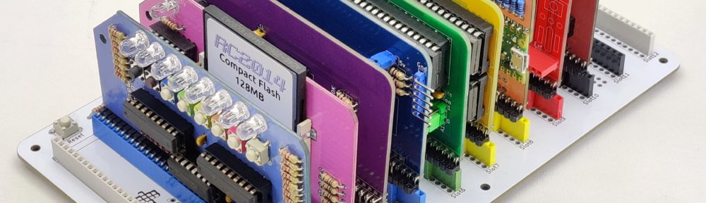
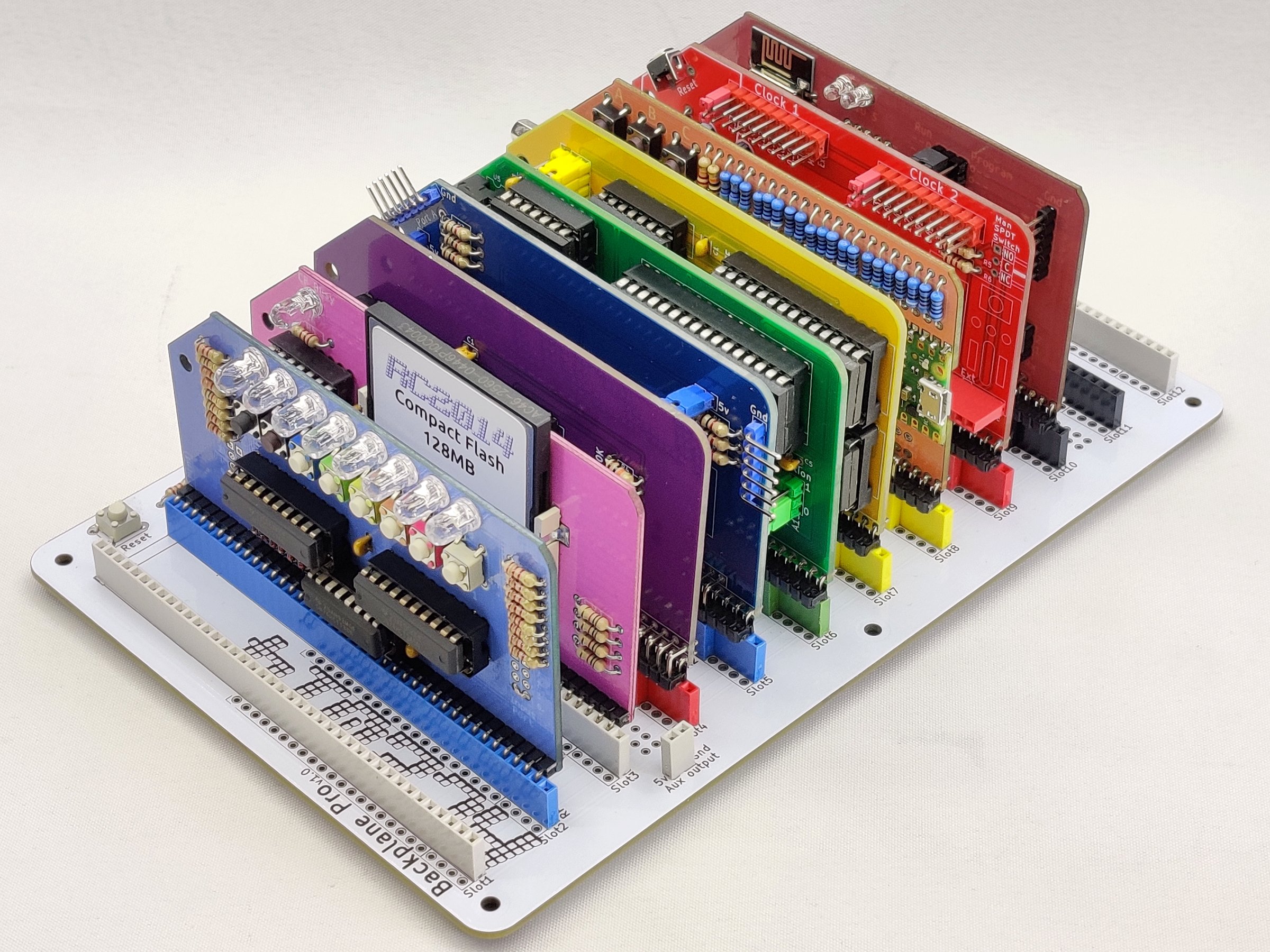
The modular nature of the RC2014 Pro, along with the vast array of colours that PCBs are available in these days has made me consider building a kit with all the colours of the Pride flag for quite some time. When it came down to it though, the colour choices were actually too limited. So I could either give up, or make the Pride Flag with the wrong colours… or find another solution.
Skip ahead to the tl;dr section if you want to jump past the theory, testing, and reasoning, and just want to see the process and settings I settled on.
Visit z80kits.com during June 2023 to buy an RC2014 Pro Pride or an RC2014 Zed Pro Pride. They are limited edition and raise money for two great Trans and LGBTIQ charities.
I started to search for different printing techniques and dye sublimation kept on cropping up, but mostly for things like mouse mats, t-shirts and mugs. After looking closer, I wondered if it was possible to use for PCBs. There are a few articles that seem to cover this, but they generally revolve around dye sublimation to make the mask to etch a PCB – and I didn’t want to go down that route! I eventually found an article by Ben Everard in Hackspace magazine which has a proof of concept. That was enough for me to dive deeper.
So What Is Dye Sublimation?
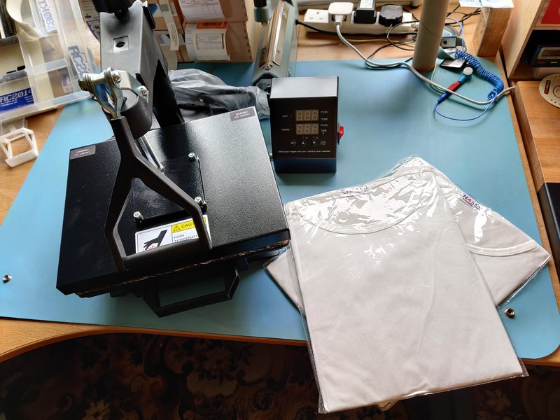
In scientific terms, Sublimation is the transition of a substance directly from a solid state to a gas state. It does not pass through the usual liquid state and only occurs at specific temperatures and pressures. The ink used for the process has this property, however, most inkjet printers cannot use this ink as they have a small heater on the print head. There are two types of printers that can be used for dye sublimation ink; dedicated printers made by Sawgrass which are really expensive, and Epson cheap crappy ones which can be converted. As Epson printers print cold, their print head won’t prematurely vaporise the ink, and conversion kits are available. Cheap and crappy is within my budget, although once the cheap printer is paired with a conversion kit, special ink, special transfer paper and a heat press, it isn’t all that cheap. All in, it was the best part of £500 investment – but I will be able to make my own mouse mats cheaply, so maybe that isn’t too bad!
The heat press is where the magic happens. With the blank (ie mouse mat, t-shirt or PCB) in contact with the ink on the transfer paper, applying pressure and heat will turn the ink in to a vapour that embeds itself in the blank. Once cool, it remains permanently* in the blank.
Initial tests
The article from Ben Everard said that he got his PCB covered entirely in white silkscreen, and it worked. Before ordering any PCBs, I wanted to try things out with some old scrap boards. I used a colourful printer calibration page to see how things came out. Obviously trying to dye blue boards didn’t work out great with the colour, but it was a lot better than I’d expected.
The thing that I was most relieved about was that the dye does not get absorbed by the metal. Yeah, it makes sense when I think about it, but a worry was that I’d have to mask off every component hole or else design the print around the holes and line it up super precisely. But that wasn’t a worry.
Even more important was that I was able to solder to the board and that the dye wasn’t conductive. More testing and things were looking good.
I had a couple of scrap boards with white solder resists, but the colour didn’t seem to work out too great.
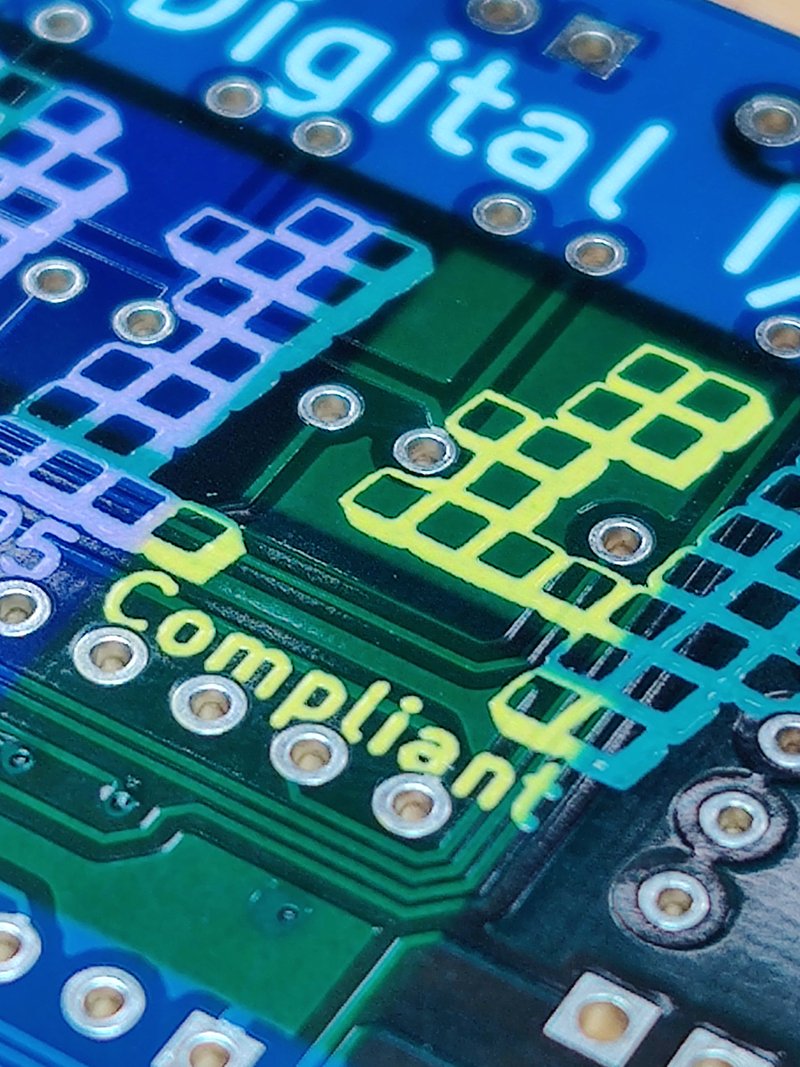
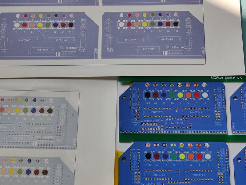
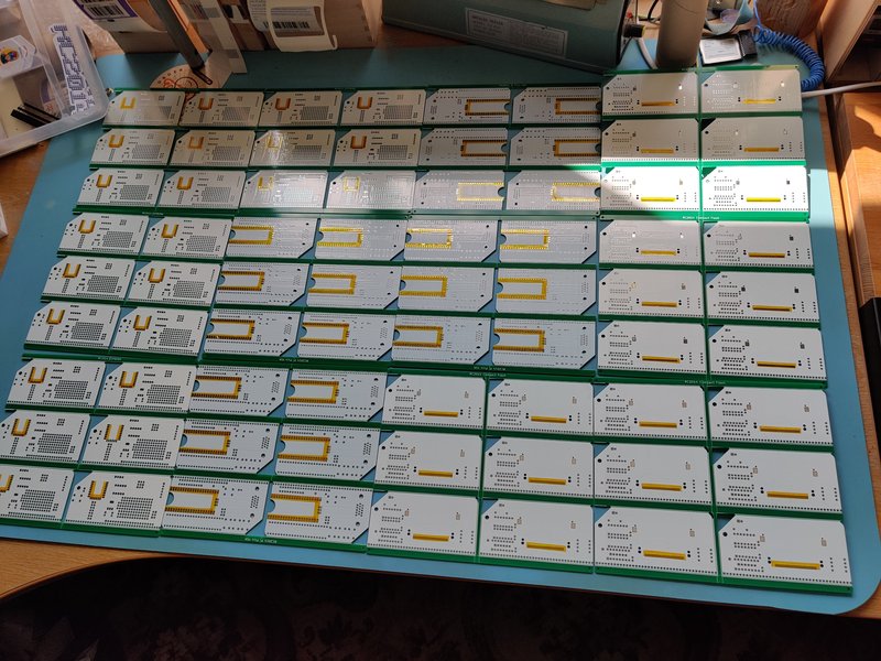
Here a real PCB is compared to a printed image of that board on to white solder resist. It has taken the dye, but really not very deeply. To test things properly, I needed some boards specifically for running tests like this. So I ordered some boards each with white solder mask and no silkscreen and some that were totally covered on both sides by silkscreen. (Fun fact: I paid to have the batch number removed on the one with no silkscreen, but I figured there was no need for that one the one which was 100% silkscreen. Turns out I was wrong!).
After exporting the original silkscreen layer from KiCad in to Inkscape I set up some different colours and tried 8 different variations between the two types of board
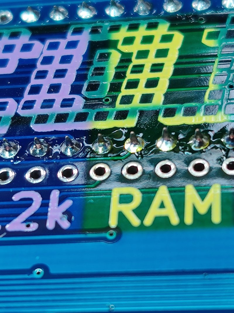
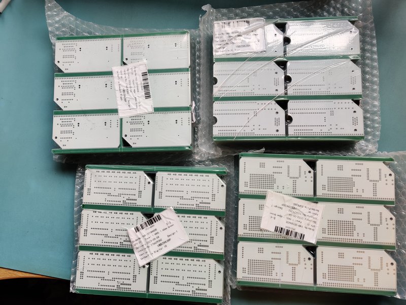
This confirmed my suspicions that the solder resist only boards had a sharper image, but they didn’t take the colour anywhere near as well as the ones covered entirely with silkscreen. As the entire motivation behind the RC2014 Pride was colour based I now had a plan. 100% silkscreen coverage for the 4 modules that JLCPCB didn’t offer the colours for; Digital I/O (light blue), Compact Flash (pink), Pi Pico VGA (Orange) and ESP8266 Wifi (brown). Of course, for the full pride flag, there should also be a black module too – however, I was able to source all of my ICs in black, so the representation is there!
To make efficient use of the dye sublimation paper and heat press bed size I decided to panelise the boards in a 2×3 grid. The KiKit plugin for KiCad does a great job of this once you’ve dialled your settings in right (Spoiler: I didn’t quite dial them in right, and there’s a very slight lip on the top where the 45 degree and radiused corner meet the top. Sorry)
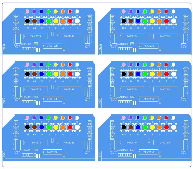
The original silkscreen layer and edge cuts from the panels was exported from KiCad in to Inkscape. From here I created a new layer above the imported layer and from here I could trace around the PCB shape and make my own artwork for it without being constrained to a single colour, font or any of the KiCad limitations. The Digital I/O module has the best representation of colour use, indicating which LEDs and switches go where. However, every board got its own bit of design flair.
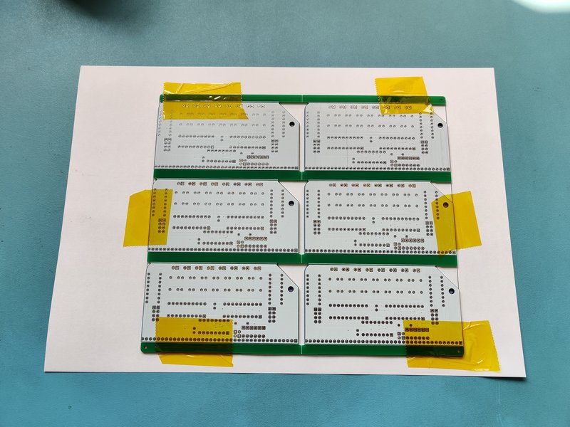
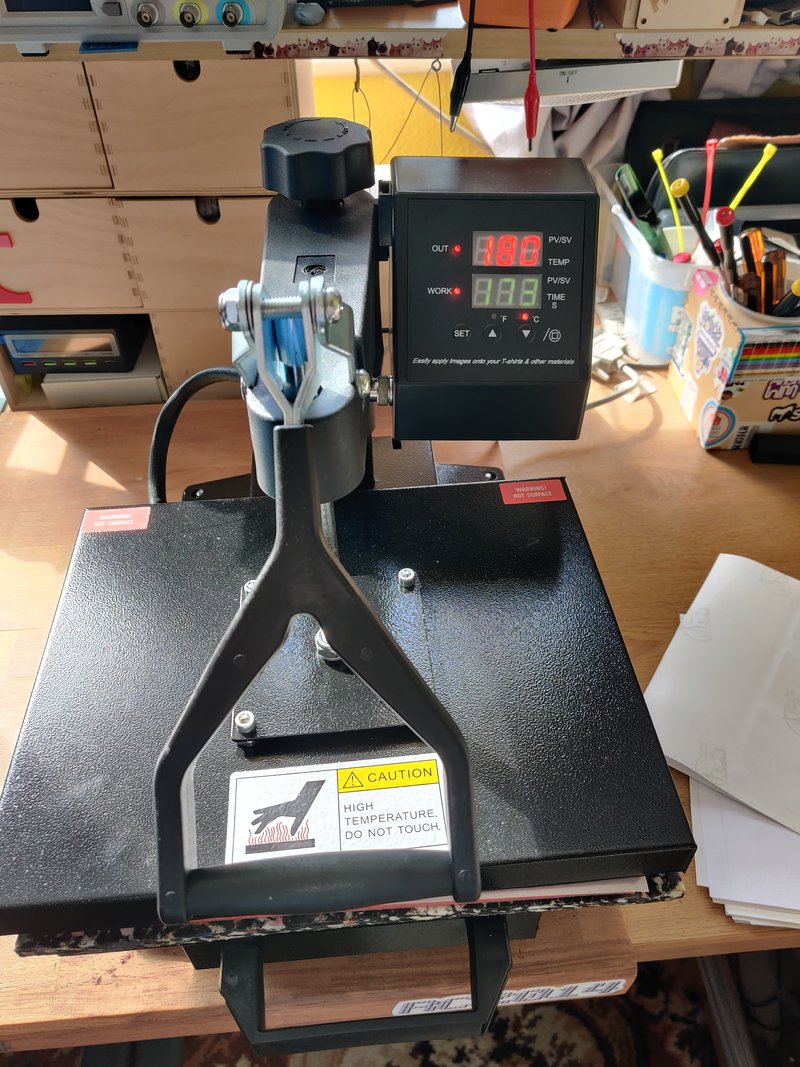
With the printer set to high quality print, slow speed and mirrored, this is then printed to the transfer paper. The PCB panel needs to be aligned very carefully and held down with Kapton tape before going in the heat press, sandwiched between 2 sheets of Teflon. Trial and error on the settings earlier suggested that 180’C and 180 seconds worked best.
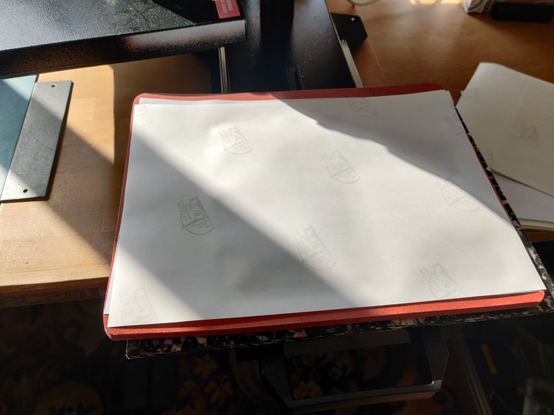
Here you can see an unused printed sheet at the top, a used sheet on the left and the dyed PCBs on the right. The colours on the unused transfer sheet are not representative of the final colour, but a .ics (image correction setting) file specifically for this ink and paper combination takes care of this and prints what is needed to get the colour you expect. You can see that some dye is left on the sheet after it has been used. Printing on to more absorbent items like mouse mats or t-shirts there is almost nothing left on the transfer sheet.
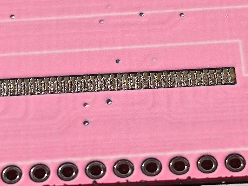
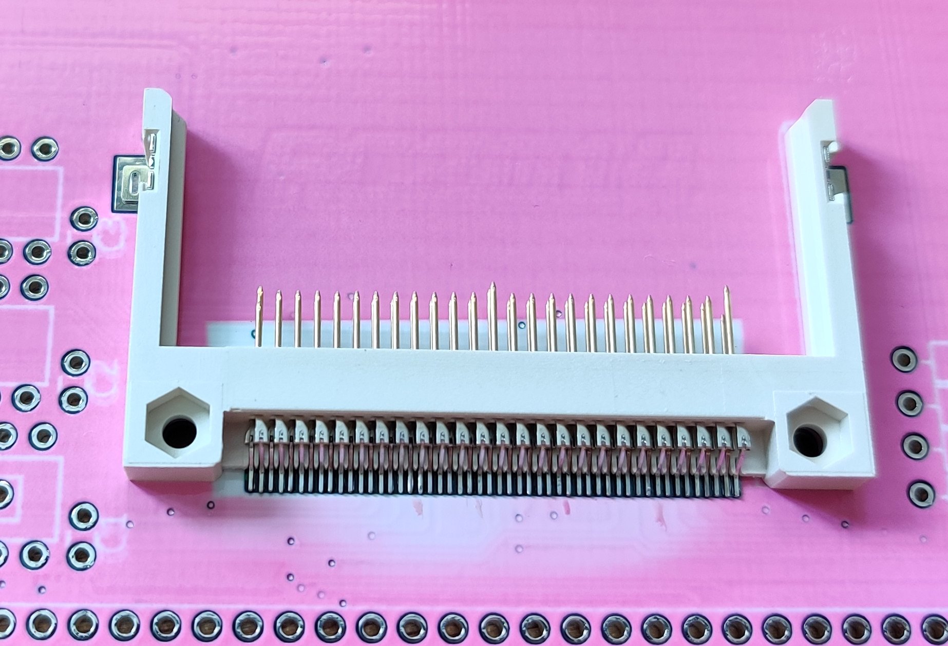
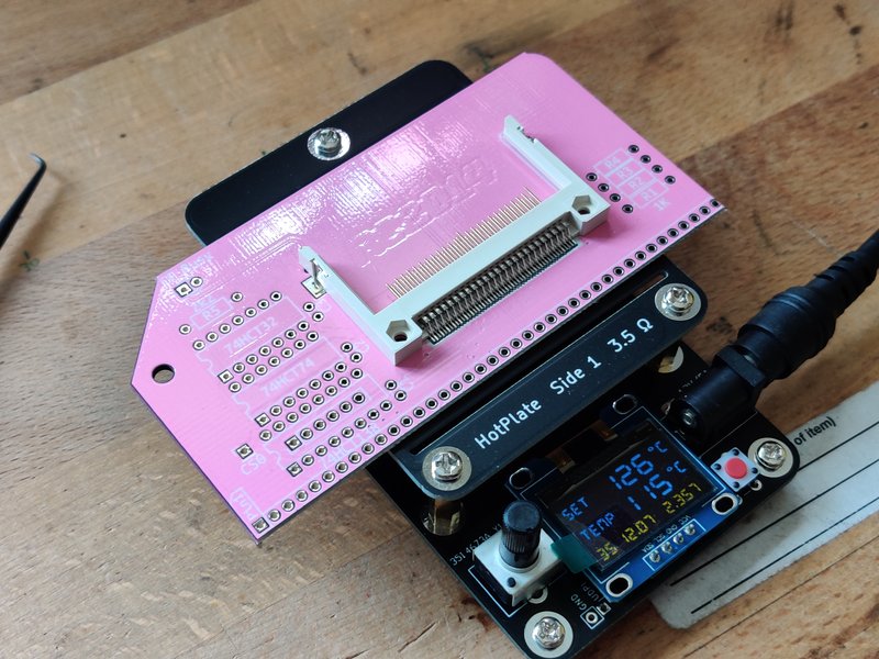
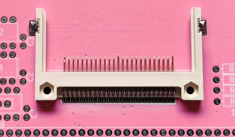
When I did the Compact Flash Module though, I encounter two big problems. When I supply the CF Modules I solder the surface mount socket beforehand as some people struggle with the 50 pin fine pitch connector. I use solder paste and a stencil, then a hot plate and hot air to reflow it.
Because the dye does not penetrate the plated pads, I assumed (wrongly) that this would be fine. However, I found it impossible to get the solder paste to stick to the pads. I don’t know exactly why this is, but I assume that the heat press somehow damages the plating. It may work better with ENIG plating, although I haven’t tested this.
I did find that a strip of Kapton tape fixed this problem, although it does add extra cost an labour to each board.
The other problem is heat. Using a MHP30 hot plate at 250’C under the board will leave a white 30x30mm square on the back where the dye has evaporated! Using hot air from above will evaporate the dye too!
The solution I found was to use a combination of a hot plate set to 125’C to pre-warm the board then the hot air only needs to spend a few seconds from above which is enough to flow the solder but only produces minimal evaporation around the socket. It isn’t ideal, but this part is hidden deep inside the RC2014 so isn’t exactly an eyesore!
The Pi Pico and ESP8266 modules are wide pitch surface mount parts, and although these seem to flow just fine with a regular soldering iron, I have played it safe and Kapton Taped over those connections too before going through the dye sub process. It adds quite a bit of time to the process, but feels important.
However, if you were doing a modern PCB with all surface mount parts then I don’t think it is feasible to use dye sublimation. Masking off every pad would be a nightmare, and there’s no way it would survive a reflow oven. So this isn’t a miracle solution that will give everybody gloriously colourful PCBs :-(
Another issue I came across was ghosting of the text. If you look at the first CF socket photo you might spot that the text isn’t too clear, although the lines are fine. The artwork was created in Inkscape on a Linux machine, but due to printer driver issues, I printed from Inkscape on a Windows laptop. I’m not exactly sure, but I suspect that there’s some kind of font incompatibility between the two machines. The workaround for this is to export as a PDF on the Linux machine with the “Convert Text To Path” option set. This PDF can then be printed from the laptop from Inkscape and the text is fine. I think this is just an issue with my setup and not anything inherently wrong with dye sublimation.
tl;dr Here’s How _I_ do it
Design the PCB in KiCad as normal, then cover the front and back with a filled in rectangle of silkscreen. Send this to JLCPCB to have the boards made
Remove the rectangles and export the front and back silkscreen layers with edgecuts to PDF file
Import the PDFs in to Inkscape. Add another layer above and use this to trace your board edge, component layout and text as you wish. Different fonts and colours and images can all be added here if required.
I exported this to another PDF then used Inkscape on a different machine to print this (this should be a redundant step though). Printed using high quality setting, mirrored and with fast mode turned off. Separate pages are printed for the front and back of the board.
Epson W2010 wireless printer has been converted to dye sub printing with a kit from City Ink Express, using their ink and paper
The white PCBs are prepared with Kapton tape over surface mount pads. Then the board is laid over the back image, aligned very carefully and held in place with Kapton tape.
The pre-heated heat press is set to 180’C. The PCB is set face down with the printed page on top, and a sheet of Teflon over the top. This is then pressed for 3 minutes then removed.
When cool, the PCB is removed from paper, flipped over and attached to the front image sheet and the heat process is repeated.
Problems and lilmitations
Whilst this offers a lot of possibilities with PCB design, it is far from perfect. Firstly is the upfront cost of the equipment needed to print and transfer the design. It is a very labour intensive process which uses specialised ink and paper, so these costs need to be taking in to account too. Alignment needs to be accurate too (unless you have a design that doesn’t need to be aligned). The image is not pin sharp, and there is a certain amount of feathering around edges due to the silkscreen, so fine details may not work too well. And lastly, the surface mount limitation is going to make it a non-starter for a lot of projects. But, with all those points in mind, if it works for you, the possibilities are endless.
It has come to light that the voltage regulator in the kits for the ESP8266 Wifi Module sent out between mid-June 2022 and 10th September is incorrect.
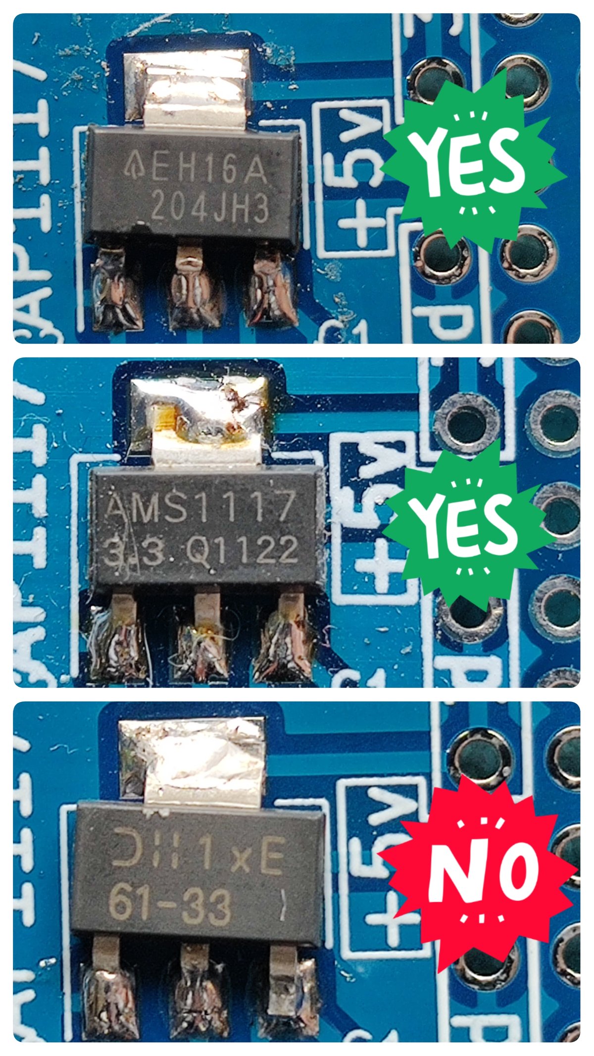
Voltage Regulator Identification
The original part, labelled AMS1117 (or similar) is a 1A 3v3 SOT-223 voltage regulator. This part was unavailable earlier this year due to the worldwide component shortage. It is a fairly generic “jellybean” component, and there are dozens of other parts that will do the same job, so that wasn’t a huge concern.
The supplier I used had a recommended replacement of a AP7361-33E (labelled 1xE 61-33). This is a 1A 3v3 SOT-223 voltage regulator, at only slightly higher price than I’d paid months before for the AMS1117, so looked like an obvious substitution.
However, the thing that I failed to check was the pinout. The SOT-223 footprint is exactly the same, but pin arrangement is different, so it causes a virtually instant short on the supply rails.
I have written to all customers that bought an ESP8266 Wifi Module between these dates, and a replacement regulator has been sent. This regulator is an AZ1117 (labelled EH16A 204JH3 or similar) and is likely to be the part used going forward.
If you received an ESP8266 Wifi Module kit before June 2022 then it should have the original AMS1117 and you have nothing to worry about.
If you received an ESP8266 Wifi Module kit after September 2022 then it should have the new AZ1117 and you have nothing to worry about.
If you received an ESP8266 Wifi Module kit between these dates, please check the part number on the regulator in your kit. If it says 61-33 then you should have had an email from me and received a replacement in the post. Please feel free to get in touch if this hasn’t happened or you are unsure.
Please accept my apologies for any inconvenience this may have caused. I take great pride in sending out the correct components with all RC2014 kits, but occasionally errors occur.


