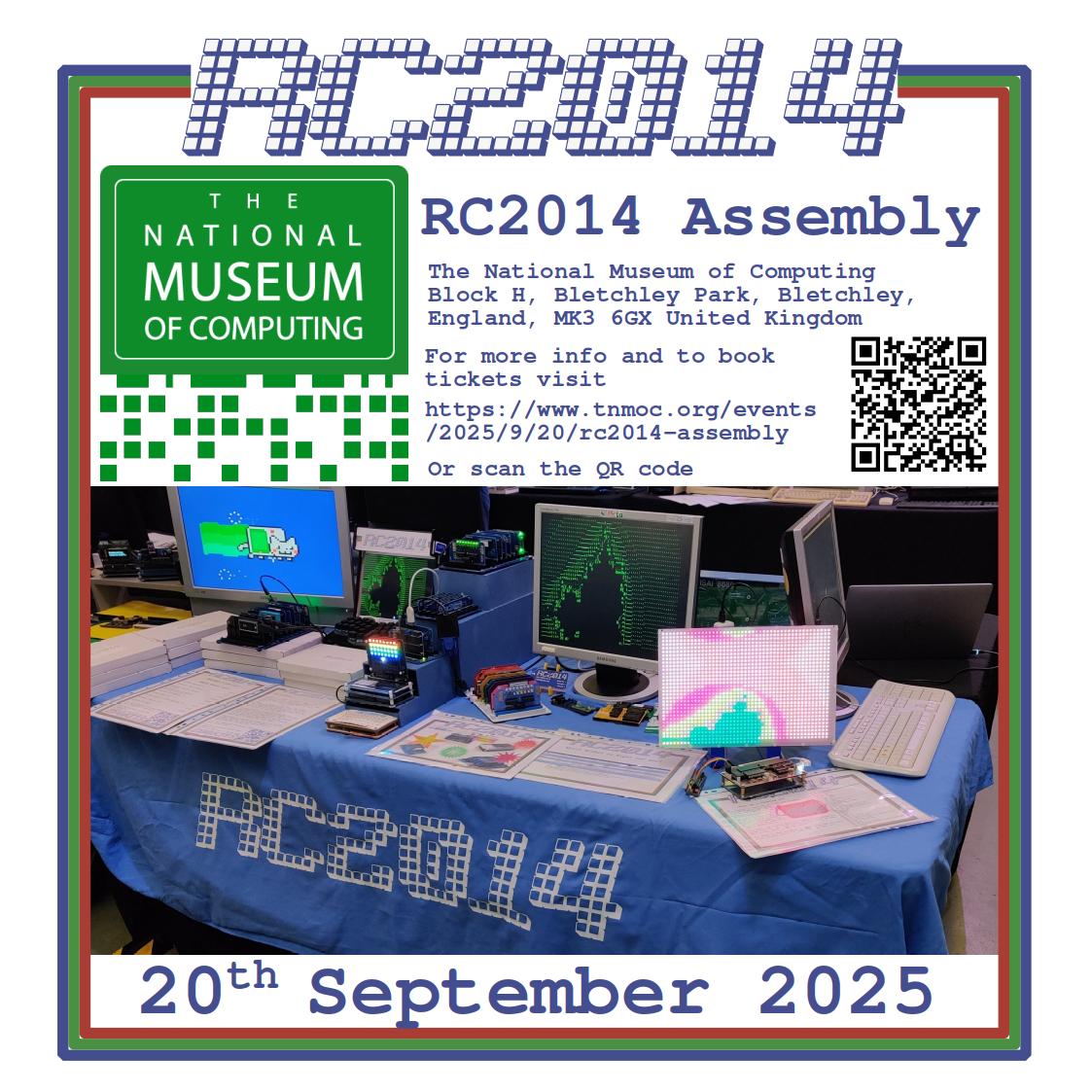
This September The National Museum Of Computing will be hosting the RC2014 Assembly. The first all-day event showcasing the RC2014 and similar modern retro computer kits.
There will be demonstrations of various hardware and software, lightning talks as well as related kits available from various vendors. Meet and chat with other RC2014 users as well as some of those that have helped make the RC2014 what it is today.
If a day of seeing/talking/hearing about RC2014 isn’t enough, the ticket also covers access to the TNMOC itself which houses the world’s largest collection of functional historic computers and World War II machines, including Enigma, Lorenz, the working Turing-Welchman Bombe, the rebuilt Colossus (the world’s first electronic computer), and the WITCH (the world’s oldest working digital computer)
Tickets for the day can be booked on Eventbrite here
There are separate tickets for Exhibitors, Traders and General Attendance. The Exhibitor and Trader tickets include a table with power, free tea & coffee, and the option to set up late on Friday afternoon (with a possible pub trip on Friday night!) and an awesome RC2014 themed name badge :-)
Feel free to get in touch if you want to discuss your exhibit or anything else about the event.
Like many small businesses, RC2014 started as a personal hobby project. When there was an interest in the PCBs it was easy enough to sell those out of a spare bedroom. As things started to take off in 2016 I set up a limited company, RFC2795 Ltd, to manage the financial side of things. Gradually RC2014 started to take over more of the house for stocking kits and components, building prototypes, and packing/shipping kits.
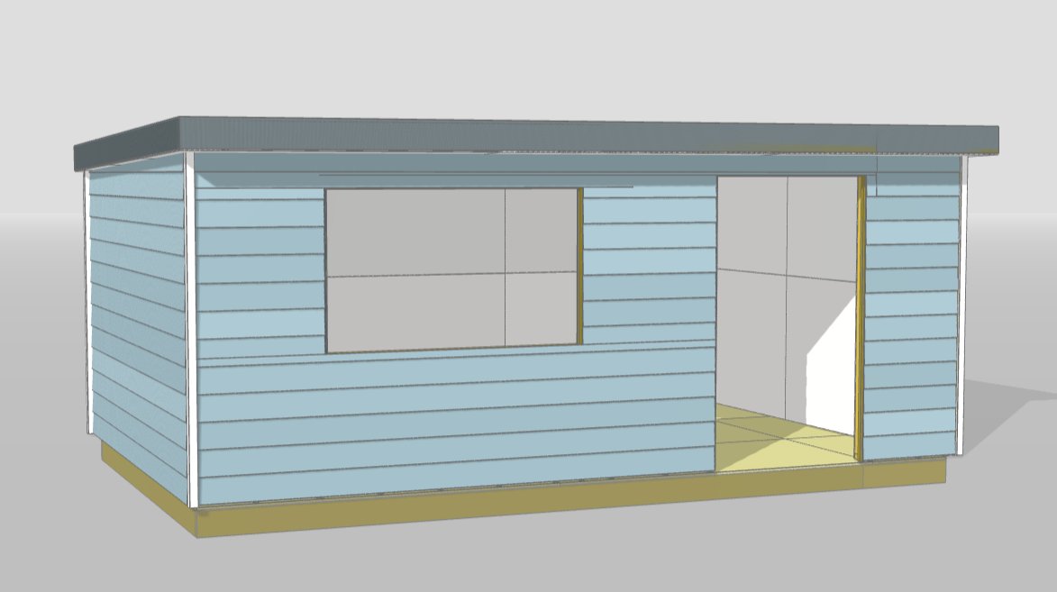
With space in the house getting more and more limited I looked in to the next step. Maybe renting an office? Rent a workshop? Move house? Buy a building for RC2014? In the end I settled on building a dedicated garden office. This allows me the home/work separation needed, whilst having minimal travel times. According to YouTube, it is something I should be able to build myself too, thus keeping costs to a minimum.
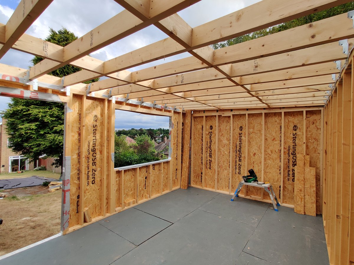
The design was a simple timber frame with flat pitched roof, large door, large window and probably clad with shiplap. The most important design aspect, however, was insulation. Lots of it. This needs to stay cool in the summer and be cheap to heat in the winter.
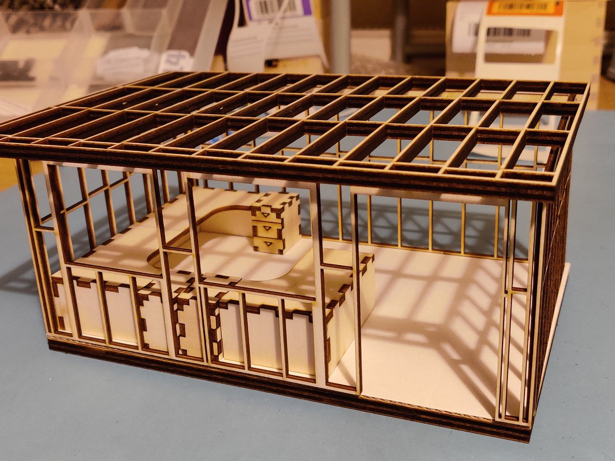
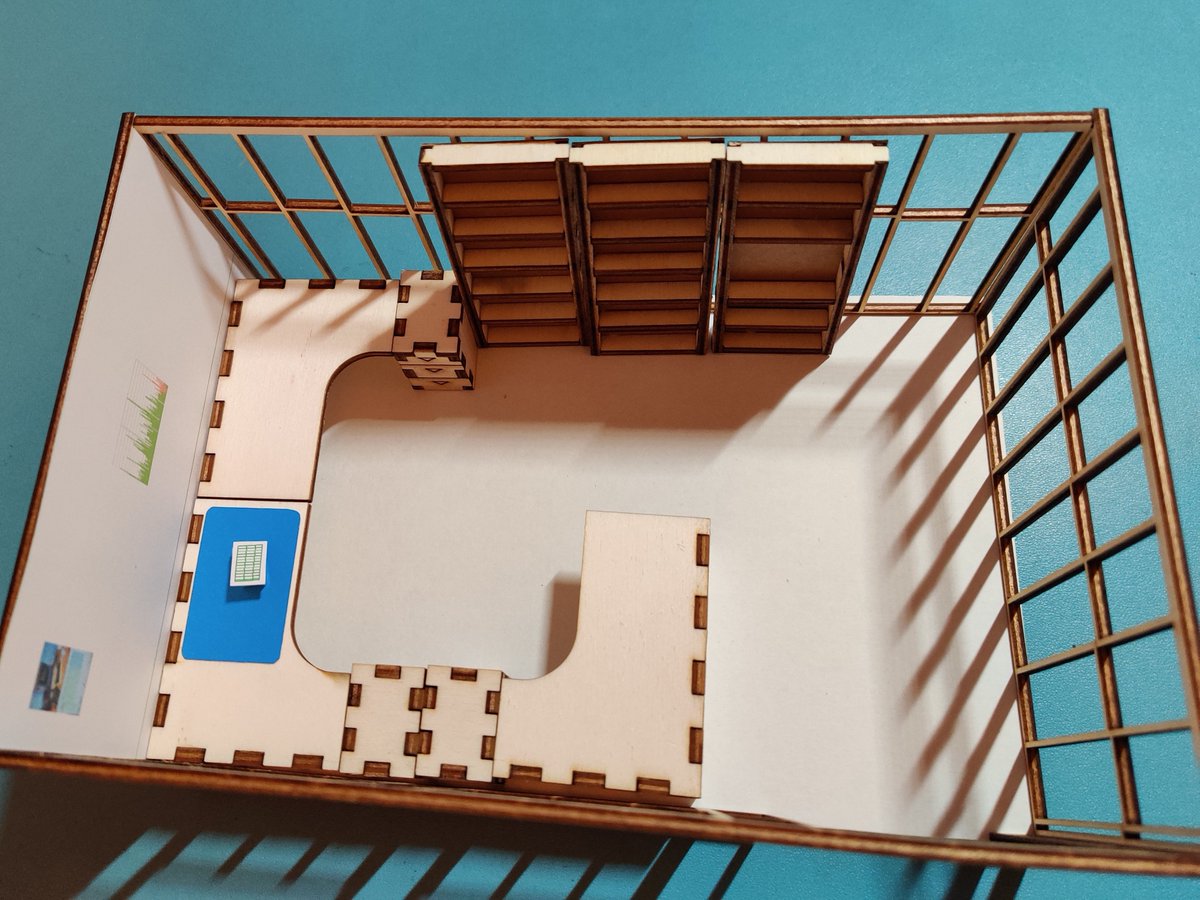
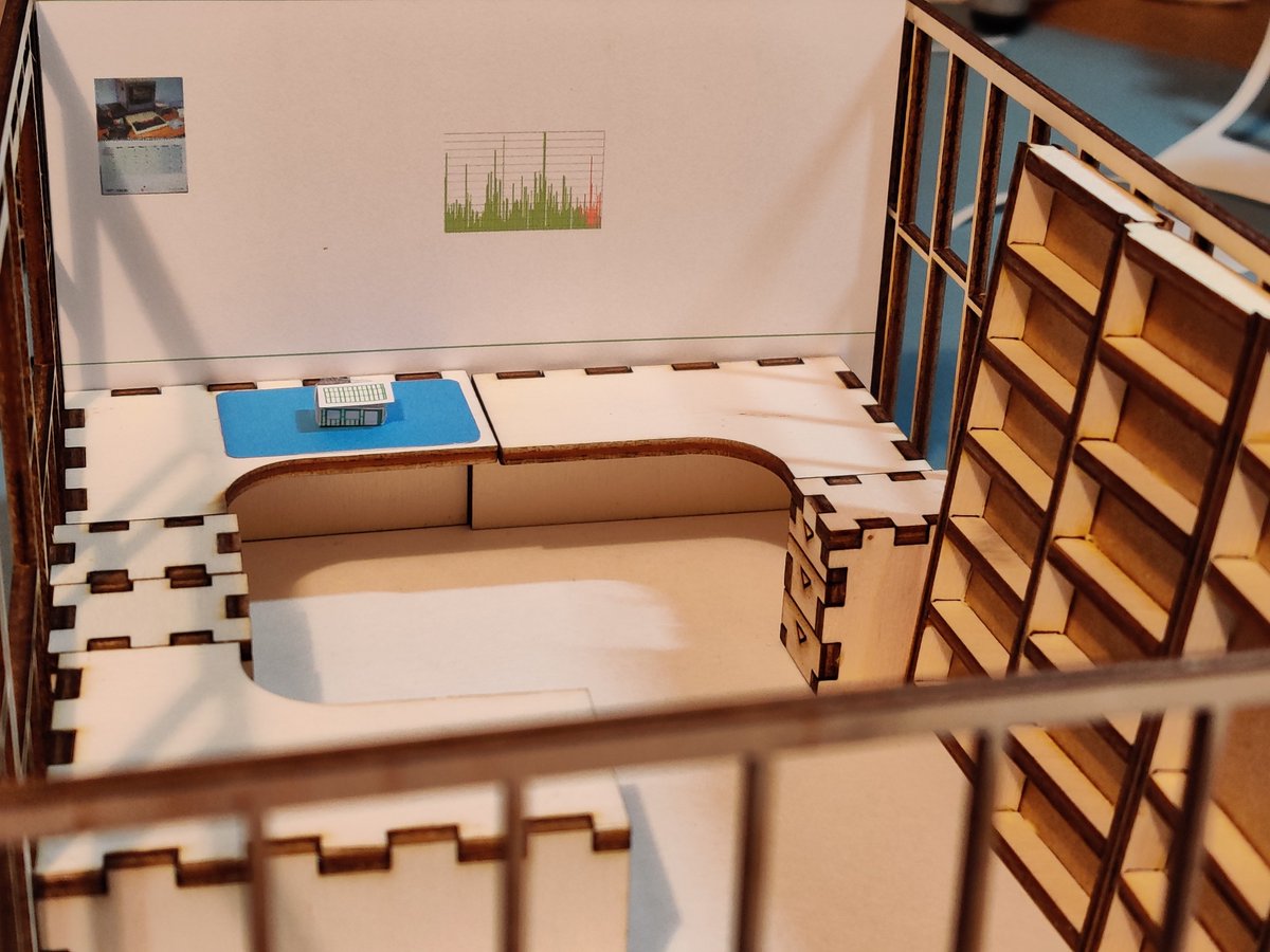
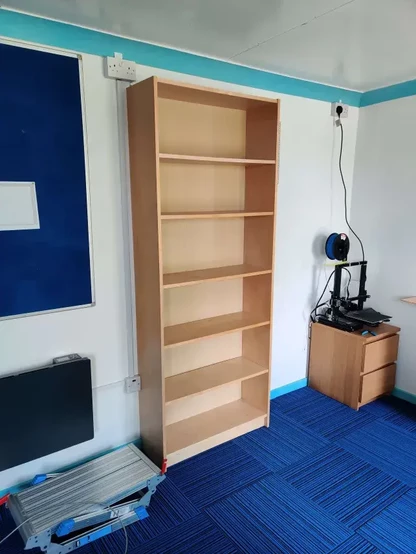
The bedroom that most of the RC2014 work is done in is 3.5m x 3.5. If the garden office was built 3.3m x 5.4m then it would be substantially larger, whilst being below the limit that would need planning application. To get a feel for the space, and see how things would work I laser cut a scale model and added scale furniture in it. Putting a scale model of the office on the desk in the scale model may have been a touch too much though!
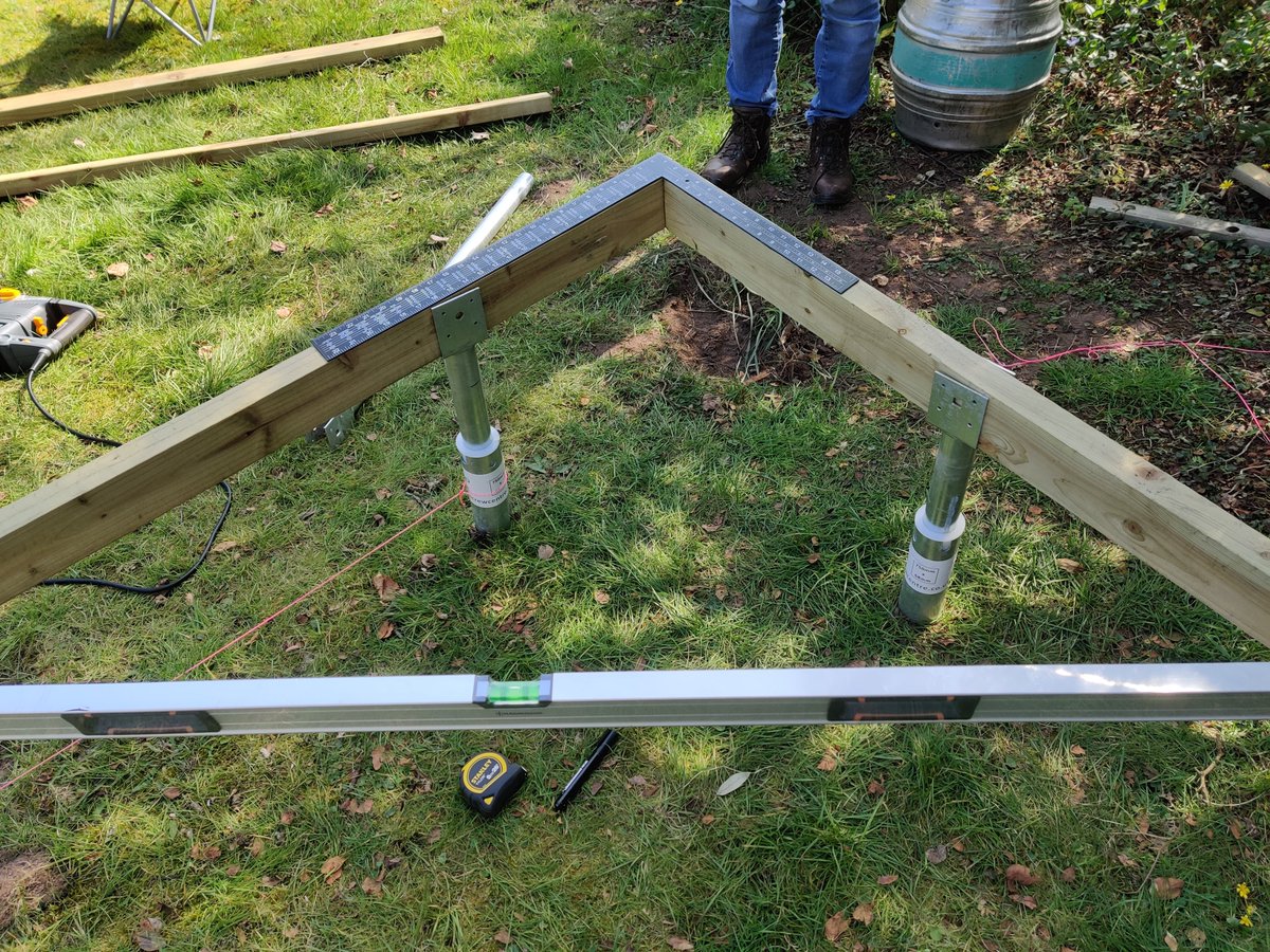
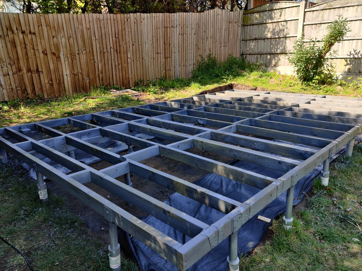
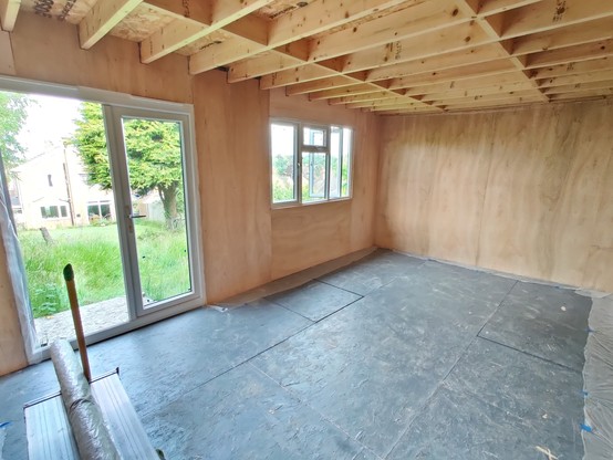
Work started in March 2022. Whilst I am lucky enough to have a garden with enough space for a garden office of this size, the garden is built on a hill which mostly slopes up from the house but also slopes right to left. This meant that in one corner the office would be over 0.5m above ground level, whilst in the opposite corner it would be about 0.4m below ground level. The subterranean corner was a lot of work to dig out, but worked in my favor because the limit on height for being exempt from building regulations is take from the adjacent ground level – thus giving me extra head height for a higher ceiling and more roof insulation. The timber frame was supported on ground screws which could be leveled out perfectly.
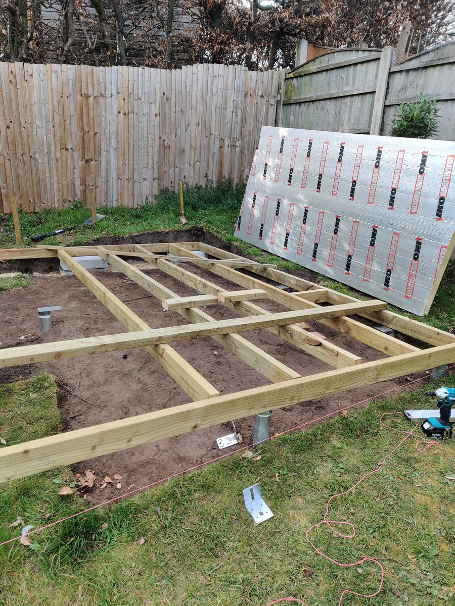
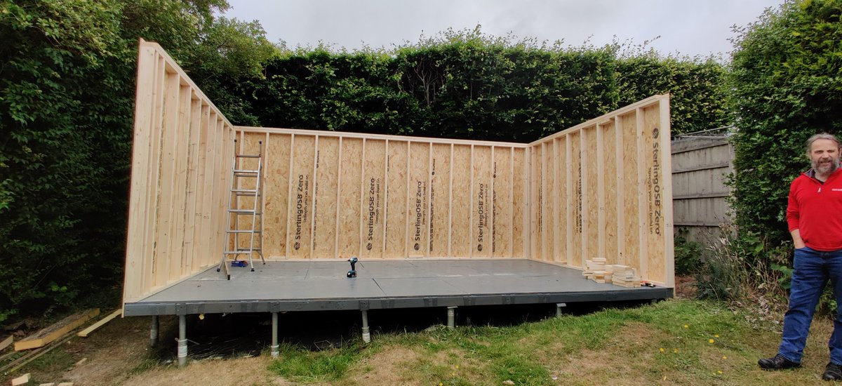
Over the very hot summer of 2022 the floor was installed and the walls erected. The elevation from road level meant great views, but carrying several tonnes of wood up to such a height was no small task. Whilst I carried out 99% of the work myself, the help of Shiela Dixon and Derek Woodruff was really appreciated.
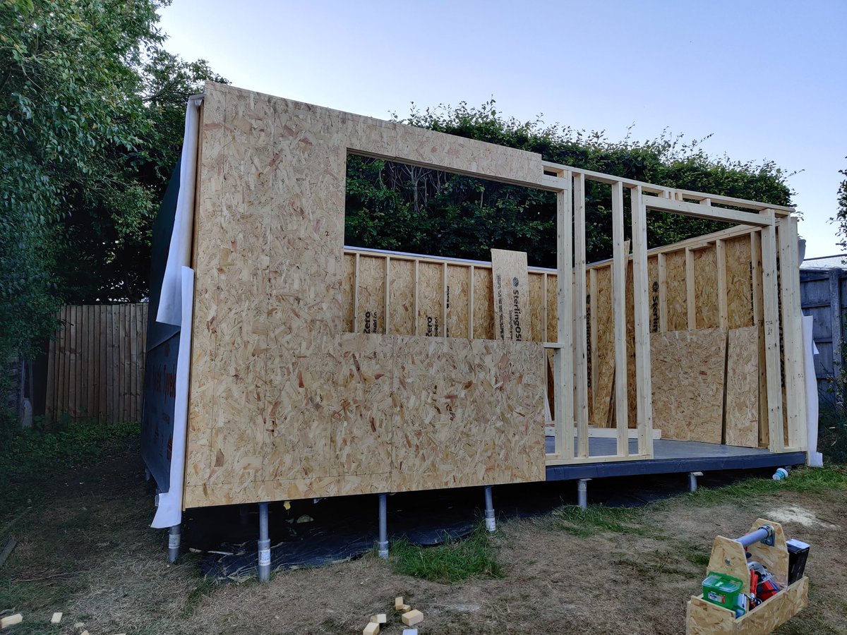
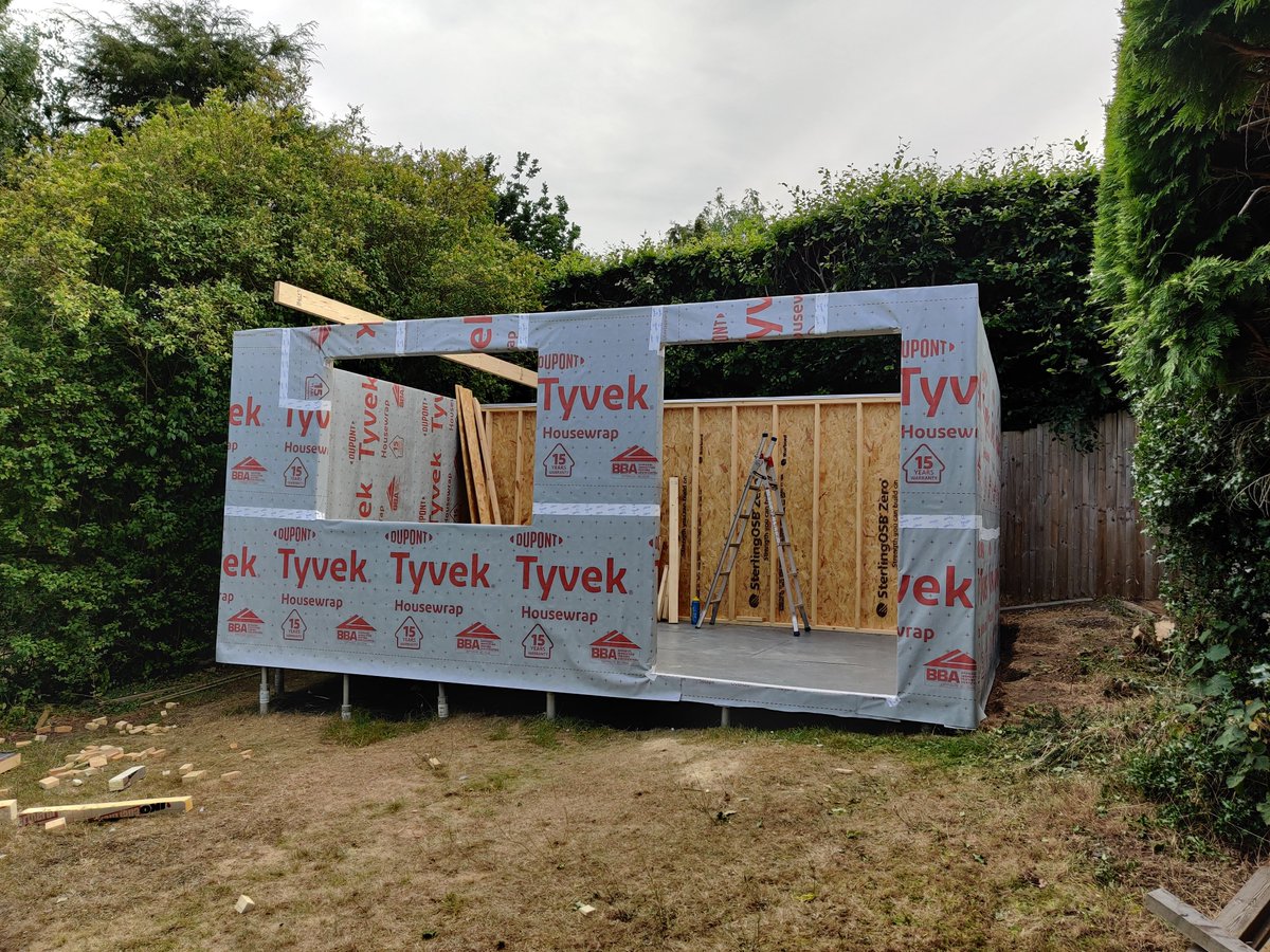
The goal for 2022 was to get to the stage of having a weatherproof box before winter. Thankfully this was achieved by the start of September.
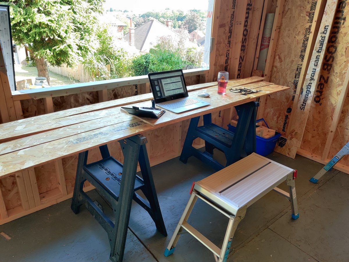
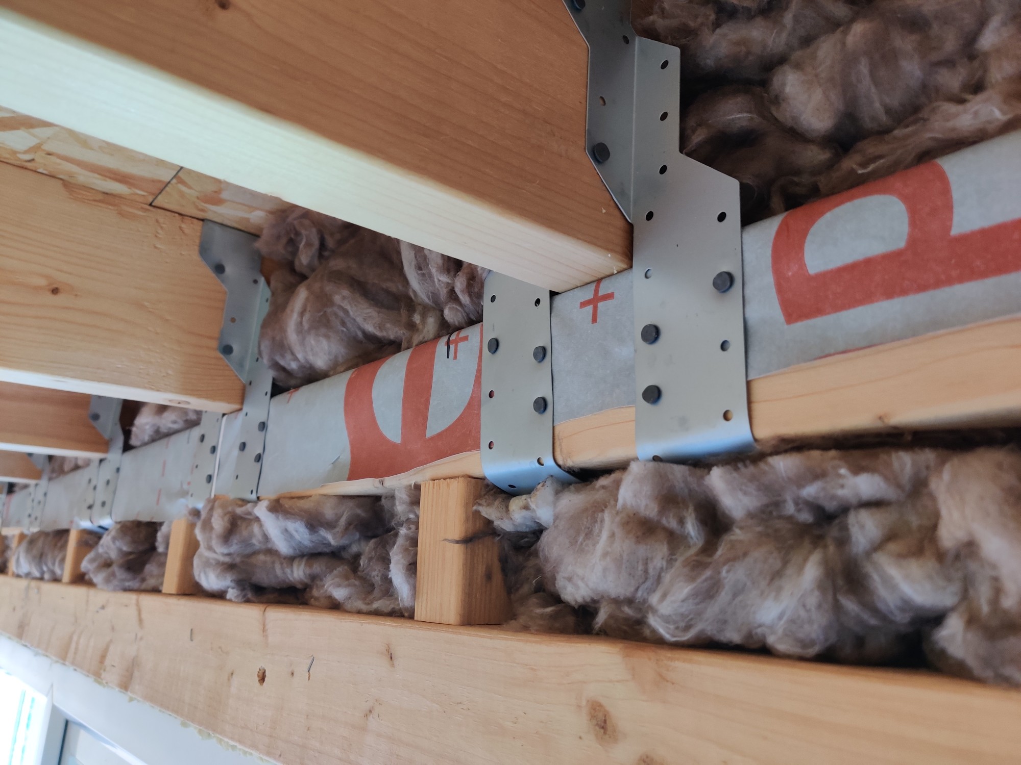
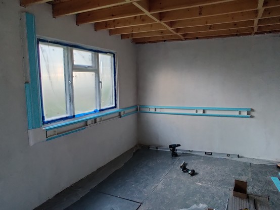
Not a lot of progress was made the following summer due mostly to a lack of time. 2024 however, saw a LOT of insulation going in before the walls were clad and painted internally.
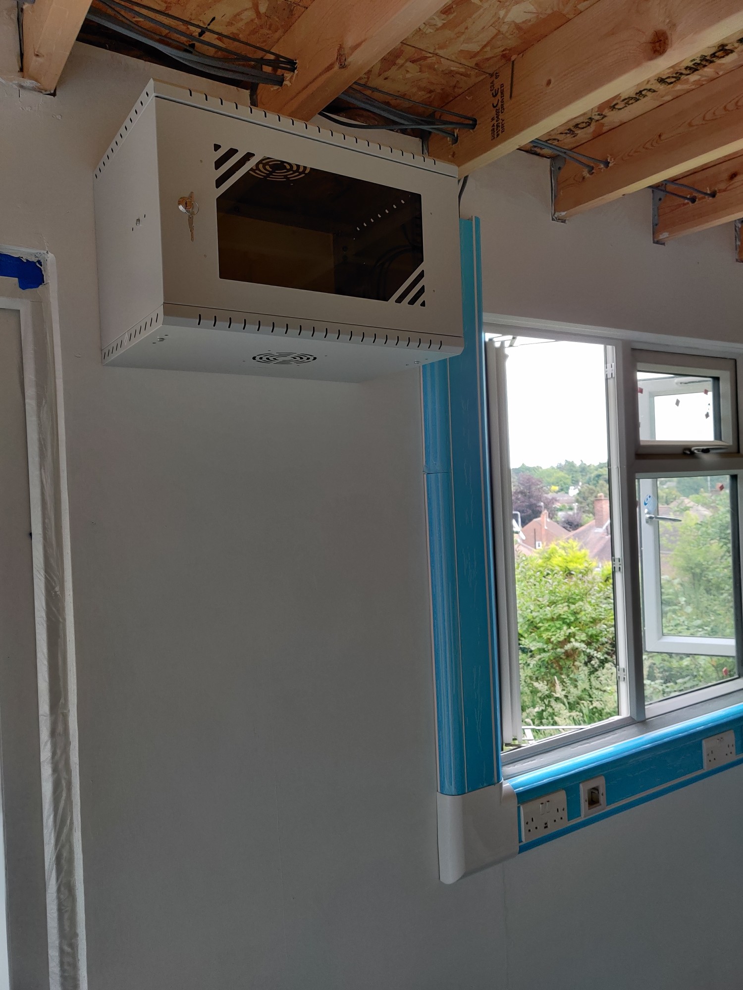
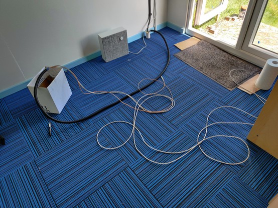
Inside the office I could run trunking and get things ready for the electrician to do his stuff. Whilst I probably could wire up the electrics safely myself, there are some jobs that I get a lot of peace of mind by paying a professional to do.
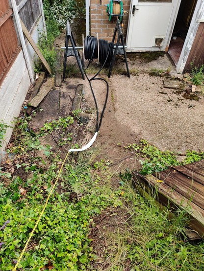
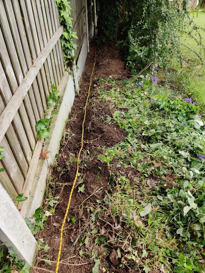
I ran the armored cable from the house to the office though, and that was much harder work than anticipated. Conduit for fiber and copper network cables was installed at the same time, but that wouldn’t be pulled through until the spring of 2025. Having power to the office was fantastic!
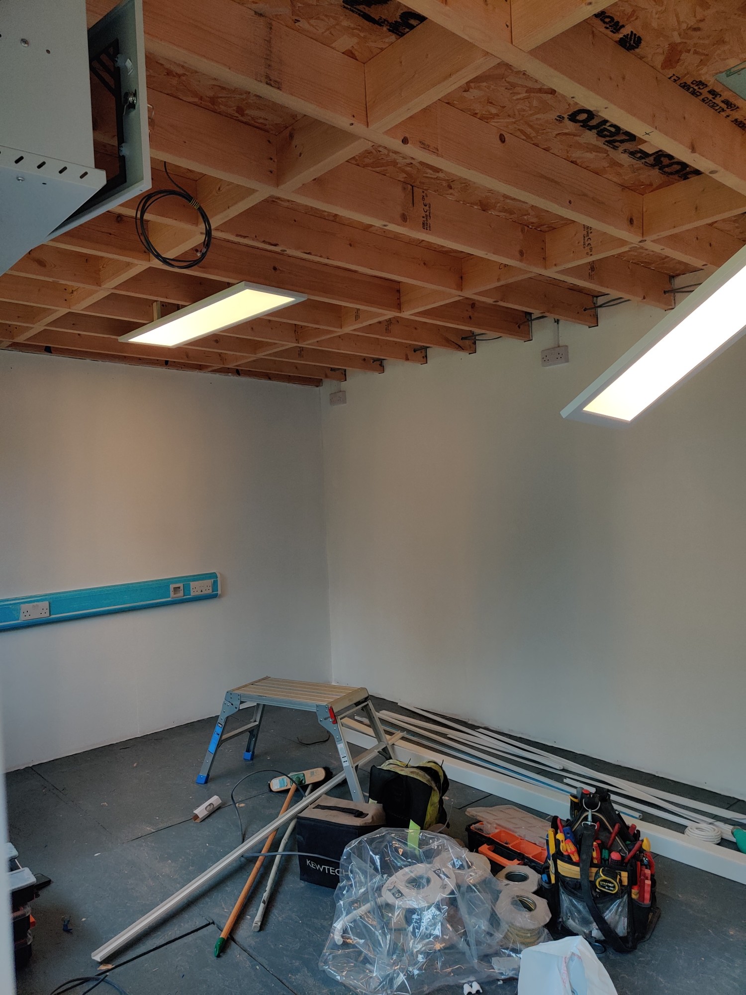
Now it was just the “easy” stuff like carpet, furniture, and moving in.
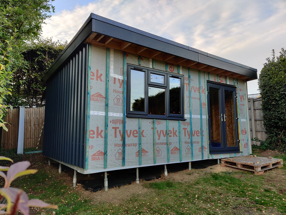
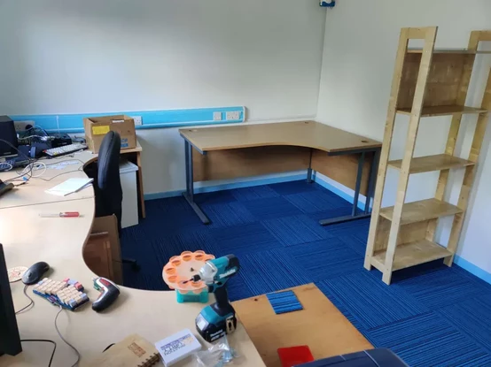
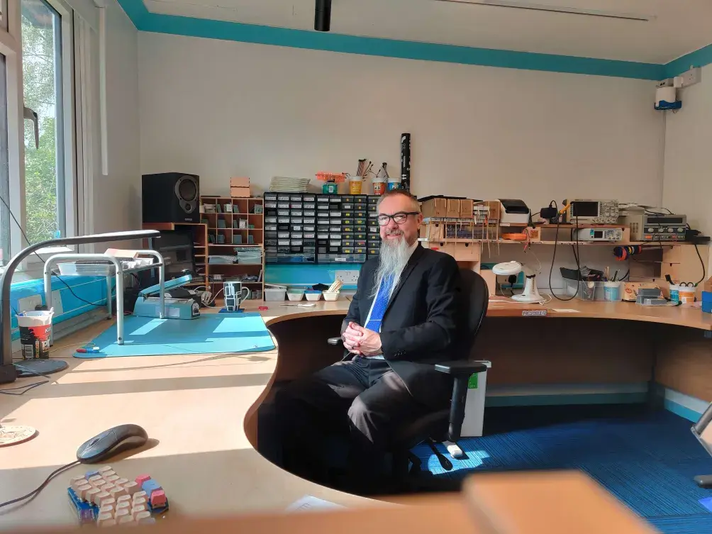
To make moving in as stress free as possible, z80kits was closed for a week at the start of June. Whilst I had been testing out the office with a few specific tasks, for the bulk of jobs it all needs to move in in one go. So everything related to RC2014 was moved from the spare bedroom to RC2014 Towers and allocated its new home in time to ship orders again on June 9th.
And there we are! Day 1 in RC2014 Towers and it is looking the neatest that it will ever look! There is 50% more surfaces to work on and 60% more storage too. This seems like overkill right now, although I know it won’t be long before I look back and wonder where all the space has gone!
When I started this build I was still on Twitter and I tweeted updates. The archive of those tweets is available here https://rc2014.co.uk/twitterbackup/rc2014towers/ (Select Browse and Oldest First for the chronological view). These days I use Mastodon, and you can follow the #RC2014Towers hashtag for updates https://mastodon.me.uk/tags/RC2014Towers
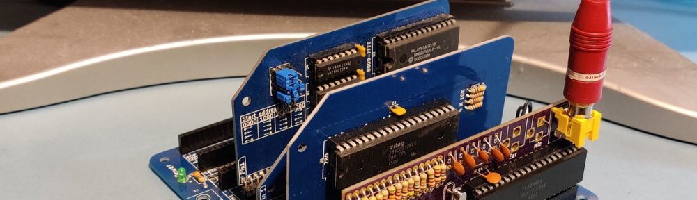
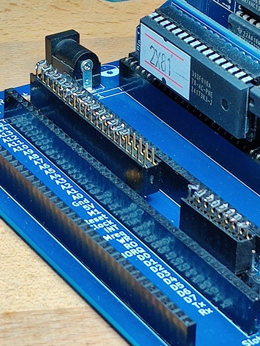
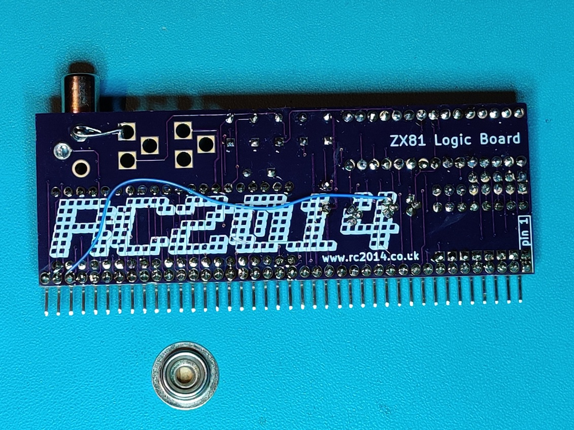
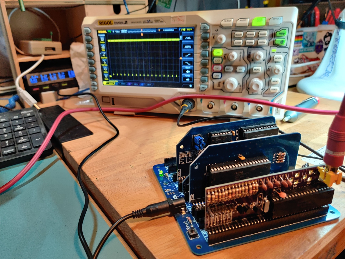
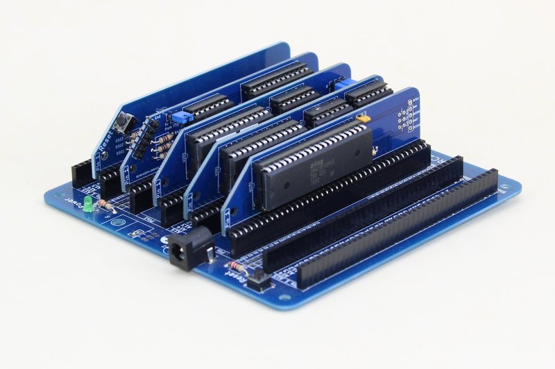
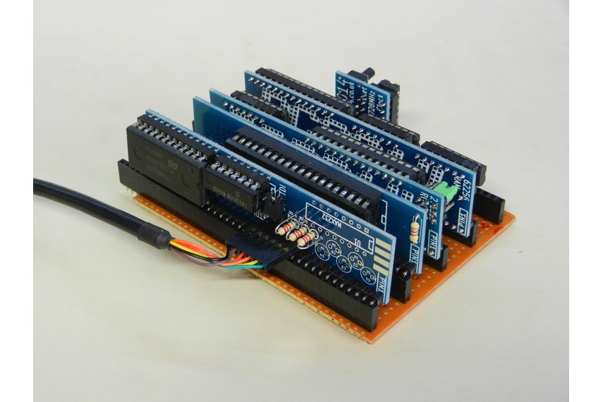
The ZX81 Module I designed in 2016 has been an example of Schrödinger’s PCB. It has sat around for 8 years in both a state of working and not working. Only when it is observed will the actual state be determined. In this wrap up post we will finally plug it in and find out.
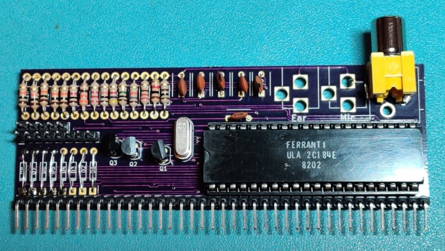
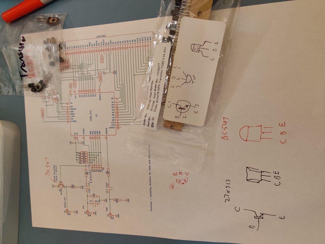
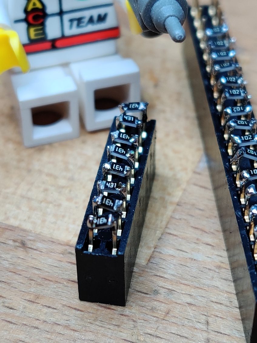
The first step was to finish assembling the board. If you remember back to the start of the month, or indeed 2016, you will have noticed that the PCB was partially assembled with 4 resistors, 2 transistors, crystal, chip socket and header pins. All the values are now on the schematic, so building up the rest of it was straightforward. I don’t know why 2016-Me only fitted 2 of the transistors. They are all the same value and I have a strip of 50 of them. I did find an error with the footprint I used for the composite jack, but this was easily fixed by turning it 90 degrees.
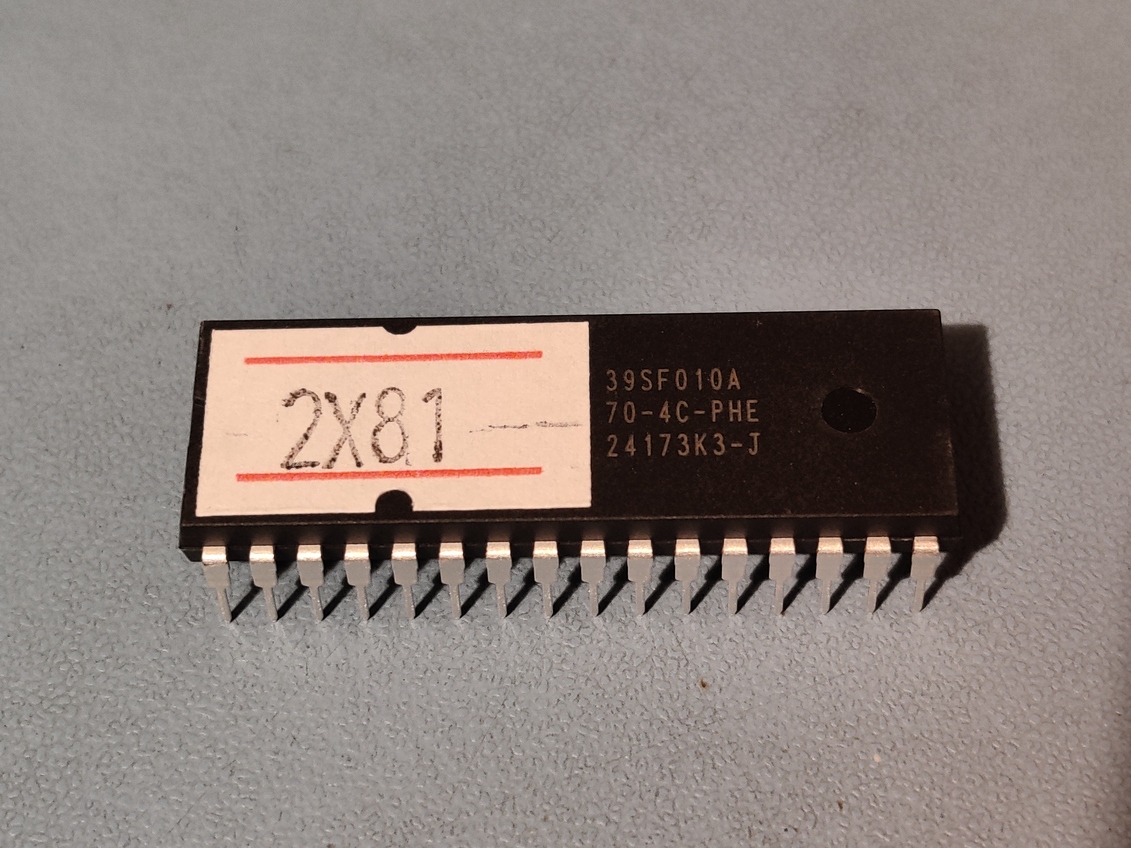
I burned a ROM with the first 8k duplicated in to the second 8k bank. Sadly my pricing gun that I use for ROM labels doesn’t have a Z, so it’ll have to be a 2X81 now :-)
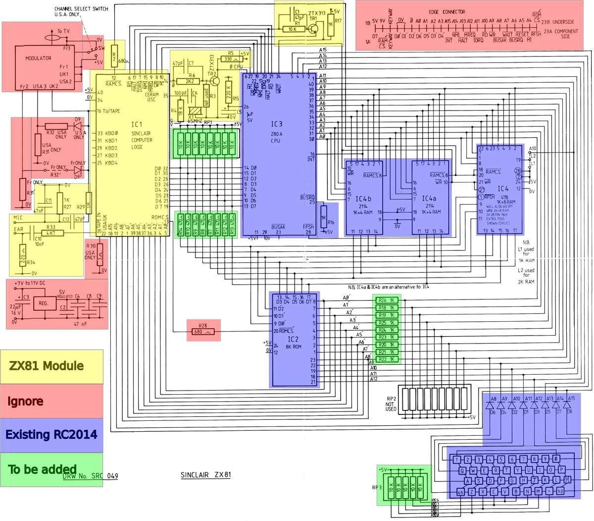
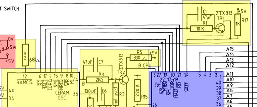
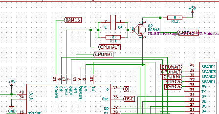
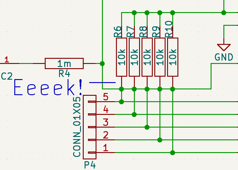
The next big dilemma was about the current limiting resistors – the green blocks on this diagram.
My understanding of what they are for is that they protect the components if there are conflicting values put on the bus. For example, if the Z80 was doing a write with 0xFF on the data bus, and at the same time the ROM was doing a write and put 0xFE on the bus. This situation should never happen, however, if it did, the D0 pin on the Z80 would be 5v and the D0 pin on the ROM would be 0v, so current would flow from the CPU to the ROM faster than the CPU could source it or the ROM could sink it. Having resistors in there will limit the current, and potentially save the parts.
The logic in a stock RC2014 means that there can only be one device writing to the address or data bus at any one time, so this kind of situation couldn’t crop up. However, with something like the original SD Memory Dump Module, the AVR chip was under software control. So any screwup on the software side could mean that both the AVR and another device could write to the bus. So current limiting resistors were important for that.
The ZX81 schematic confused me though. The CPU and RAM sat on one side of the address bus resistors with the ULA and ROM on the other side. But the CPU and ULA were on one side of the data bus resistors with the ROM and RAM on the other side. I do not fully understand exactly what the ULA does, but the implication is that it could mess with either bus in some way. The RC2014 backplane certainly doesn’t allow for that combination of modules with resistors between them. Rightly or wrongly, I decided to separate the ULA from the ROM, RAM and CUP via resistors.
Rather than solder a load of resistors to the backplane though, I put header pins on there and then used sockets with badly soldered surface mount resistors on them. That way I could swap them out or replace them with jumpers if necessary.
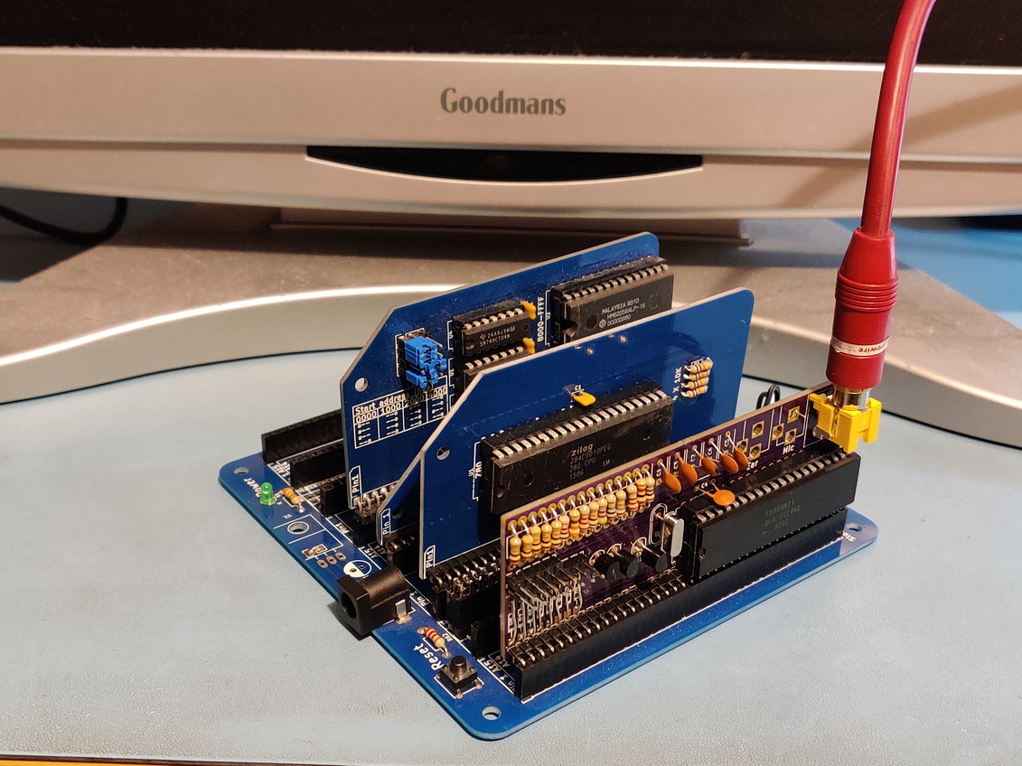
So, finally I had a completed module, a programmed ROM, backplane with resistors on it, and no more excuses for not powering it up.
So I did….
And…
Nothing.
Well, nothing with a combination of heat from the ULA. That is probably not good. I only powered it up for a few seconds, but it clearly got hotter than it should. So rather than risk doing any damage, I decided to go back to the schematics and look closely at everything on my module compared to the original ZX81 schematic.
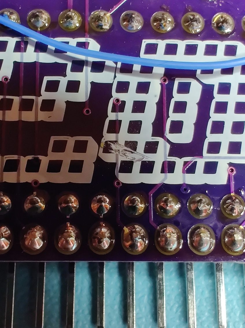
It didn’t take long before I found a discrepancy. The transistor at the top has the emitter connected to the NMI signal on the ZX81, but my module had it connected to the WR signal. I don’t know exactly what the effect of this would be, but I know it isn’t going to give the desired outcome!
Luckily the fix isn’t too difficult. One track needs to be cut, and a wire needs to be added.
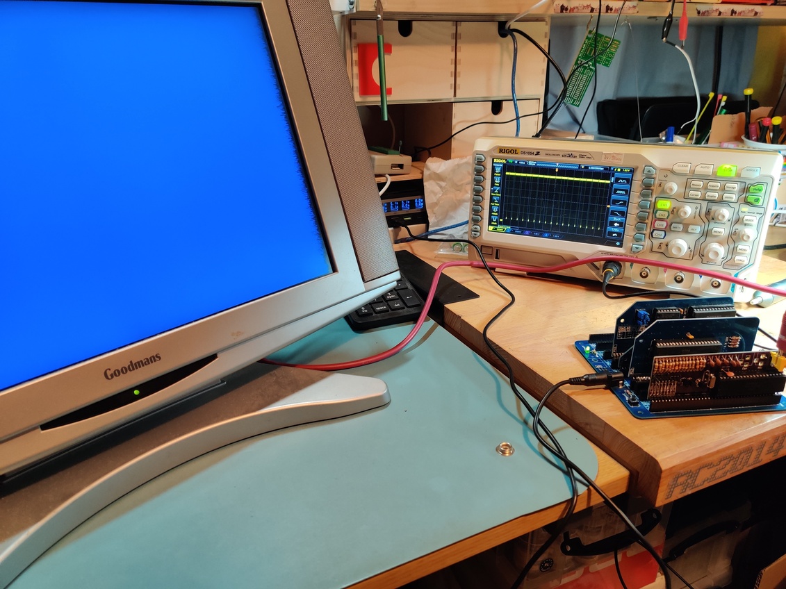
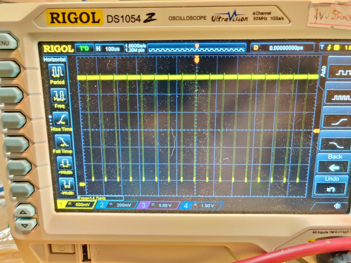
So, with that fixed, everything should power up just fine, right? Right? Sadly, no.
The ULA didn’t get hot, though. So that was definitely better. There was also a regular pulse on the composite output that looks a lot like a line sync signal. But there is nothing else.
Time to look closer at what I did in 2016. Whilst there were very few components soldered on to the PCB back then, 2024-Me assumed that those were at least correct. Which turned out to be a mistake! The ZX81 uses a 6.5MHz crystal. However, I had soldered a 7.3MHz crystal on to the board. Why? I really have no idea. I also have no 6.5MHz crystals either. The closest I have is 6MHz.
As video signal is derived from the crystal, the value has to be pretty accurate. Without the right crystal this is never going to generate a white screen with a happy little K cursor in the bottom corner. However, a poke around the data and address lines makes it look to me like the rest of the computer isn’t running either. So even with a picture being generated, I doubt it would include a K cursor on it.
Schrödinger’s PCB has finally been observed, and it is currently not working :-(
Why? I do not know. There are several aspects that might be playing a part. So for Retro Challenge 2025 I will certainly need to address these
6.5MHz crystal needs to be obtained
ULA needs to be checked. I don’t think the few seconds where it got hot killed it, but I cannot assume that it is totally undamaged.
Limiting resistors need to be understood better
Shadow copies of the ROM might need to be in the upper memory. I don’t think this is necessary, but it is a deviation from the original ZX81 design.
My decision in 2016 to base my module on a ZX81 because of the simplicity of a ULA might be flawed. In hindsight, the ZX80 might have been a much better place to start. There are a lot more chips in that design, but they are all regular 74 series logic, and each part of the circuit can be broken down and understood. That will demystify the Black Box of the ULA at least. I will leave it down to 2025-Me to decide if he wants to carry on with this module, or start afresh with the ZX80 schematic.
The schematic for the ZX81 Module I designed in2016 had been designed in a very old version of KiCad, and hadn’t survived all the upgrades too well. This resulted in every component being replaced by a question mark in a box. Luckily I had some photos of the schematic from previous Retro Challenge posts, as well as an expectation as to what should be resistors or capacitors or whatever.
Things now look much better, and actually make some kind of sense.
2016 Me didn’t consider the importance of putting component values on the schematic. Or the PCB. My module was based on the original ZX81 schematic though, so it was pretty much a case of matching up components and updating their values.
The observant amongst you will notice that the ZX81 schematic has a lot more stuff on it than my module. These changes can be categorised in three ways;
Components which the RC2014 already have, such as the Z80 CPU, ROM or RAM
Components which need to be added, but are not part of the module, such as the keyboard or data/address bus resistors
Components which will not need to be included, such as the TV modulator including the USA/French options, or power regulation.
In addition, I noticed my module design had some extra components that were not part of the ZX81 schematic.
More specifically, this is a transistor and resistor. This actually matches the composite mod that the donor machine had. So, well done 2016 me for thinking ahead and including this!
Something which is a bit more concerning though is the way that the keyboard lines all seem to be shorted against the TV Out netlist. I think this might be an artifact of the schematic rescue, as I am sure that 2016 Me would have noticed that. However, I still need to test the PCB in case this fault has made its way through to the board.
So, with a donor ULA, and all the component values, I have everything I need to finish the module. There are other important things that I need to do to the RC2014 though. Firstly, I need to burn a ROM.
You may remember from a recent post that I did a partial ROM dump from the donor machine. This was a simple BASIC program
10 FOR F=1 TO 200
20 PRINT PEEK F;
30 NEXT F
I remember reading that the ROM chips used on old machines were almost, but not identical pin out to the 27C EPROM chips, and that it was a couple of data pins which were swapped over. Or something like that. So my worry was that, for example, D3 and D7 on every byte was swapped. So if I could compare the first 200 bytes or so then I would know if everything matched, or if the difference was consistent.
Luckily, everything matched with the ZX81.ROM file I have.
Although converting decimal to hex becomes less and less fun as you go. But at least I know that I should be able to just burn that image to a ROM and it *should* work.
The memory map on a ZX81 is a ZX81 is interesting. The ROM shows up in 4 locations, and the RAM is mirrored too. A13 is the only line used to decode if ROM or RAM is accessed. Therefor the memory map looks like this;
FFFF
      RAM (Shaddow)
E000
DFFF
      RAM (Shaddow)
C000
BFFF
      ROM (Shaddow)
A000
9FFF
      ROM (Shaddow)
8000
7FFF
      RAM
6000
5FFF
      RAM
4000
3FFF
      ROM (Shaddow)
2000
1FFF
      ROM
0000
As I understand it, Only the 8 ROM from 0x000 to 0x1FFF and the 16k RAM from 0x4000 to 0x7FFF actually matter. However, my plan is to burn two consecutive copies of the ROM and set the Pageable ROM Module to a 16k bank size. I will also use a 64k RAM Module with RAM starting at 0x4000. This will mean that the shaddow ROMs from 0x8000-0xBFFF will actually be RAM. I very much doubt that anything makes calls to that address range expecting it to be ROM, but as long as it isn’t critical to bootup, I can write a routing to fill that RAM with the ROM contents.
So, with all of that sorted out… I just need to solder some components, burn a ROM, and put it all together.
Following on from the failure to get the Portfolio talking directly to the RC2014, I decided to turn my attention to the Cambridge Z88. I already have a custom RS232 to TTL serial adapter for that, and the RC2014 is all set up ready for the Portfolio at 9600 baud, so this should be straightforward…
Well, would you believe it, it was a success! The Z88 is a fantastic machine, with some good built in programs. One of those is a terminal emulator, so it really was just a case of plugging the RS232 adapter in to the RC2014, with Port B set as the primary port set at 9600 baud.
To test it properly, I typed in the test program for the LCD module https://rc2014.co.uk/modules/lcd-driver-module/ (The initial test failed, but after I plugged the LCD in correctly, everything worked fine).
Buoyed on by the success there, I decided to turn my attention back to the Portfolio. Knowing that the Z88 RS232 to TTL serial adapter worked meant I didn’t have to burn my fingers again! The only issue was that the Z88 had an almost but not quite standard pinout on the DB9
I blogged about the Z88 RS232 to TTL Serial adapter back in 2013 https://sowen.com/466/z88-to-ftdi-lead-via-max3232/ The important takeaway from this is that Gnd is on Pin7 on the Z88, although it is Pin5 on the Portfolio. It is also worth noting that Pin1 and Pin9 both carry 5v, and whilst these aren’t used in my adapter, they could break other things they are plugged in to. Pin2 and Pin3 are Tx adn Rx respectively on both the Z88 and Portfolio.
Time for a Frankenconnector to adapt them!
The other bit of unfinished business on the Portfolio was putting some terminal software on there. A copy of xterm2, as supplied on the Portfolio utility card was easy enough to find. In the past I had transferred programs to the Portfolio via the parallel adapter, however, I had recently bought an APF-01 memory card from https://apfram.com/ Whilst I had to use some propriety software on a Windows machine to copy the files on to it, it worked really well.
With everything connected up and Xterm2 started, the Portfolio and RC2014 were talking!
Again, I typed the LCD test program and sent a message to be displayed from the Portfolio to the RC2014
Although, of course, it was only as I type this blog post that I notice the Off-By-Ten error in that message! Ooops!
So, that is the Z88 and the Portfolio both ticked off of the list of computers to talk to the RC2014. Whilst the Portfolio wasn’t a complete failure before, I am really glad I revisited this and got a more satisfying result. And it has reminded me just how good both of those two machines are. I really should use them more.
If you read the intro post to this years challenge, I set myself a secondary goal of getting many of my old computers talking to my RC2014. So I decided to kick things off with the Atari Portfolio. This was going to be an easy intro in to things as this little DOS compatible palmtop has a serial port expansion and can run DOS based terminal software. So this would be pretty straightforward, right?
The Portfolio serial port is limited to 9600 baud, so this gives me a couple of options on the RC2014. I could either slow main clock right down, which will slow the CPU, but I will get 9600 baud on serial Port A. Or I could slow down Clock 2 and use Port B as the primary port. Rather than dive in headfirst and make a mess of things, I came up with a simple step by step plan;
Power up the RC2014 and check that it is all working
Plug in to PC and verify 115200 baud on Port A is working.
Connect to Port B and verify this works at115200 baud
Change Clock 2 and check the PC can communicate at 9600 baud on Port B
Install terminal software on the Portfolio
Plug the Portfolio in to a serial to USB adapter and check it can communicate with the PC at 9600
Build a simple MAX232 adapter to convert the RS232 on the Portfolio to TTL serial
Check this can communicate with PC FTDI
And, finally, connect the RC2014 and the Portfolio, via the MAX232 adapter, using Port B at 9600
The first 3 steps went without a hitch. Using Port B as the primary port was as simple as flipping a switch when using the Front Panel. However, when I dropped the RC2014 down to divide Clock 2 by 12, I was unable to communicate at 9600 baud. This didn’t bode well. In case I didn’t get the jumper right, I tried setting the terminal to 4800 and 19200, being the speed just above and below 9600, but to no avail. Anyway, long story short, I wasted an hour before discovering that indeed the jumper was of by one, but it gave 14400 baud, which my terminal software didn’t support! So ok, progress, but slow progress.
On to the Portfolio. I plugged in the Serial Port expansion, connected a RS232 to USB adapter, and plugged it in to the PC. Using the DOS command COPY AUX CON meant that whatever I typed on the PC came out on the Portfolio screen, and COPY CON AUX meant that whatever was typed on the Portfolio appeared on the serial terminal.
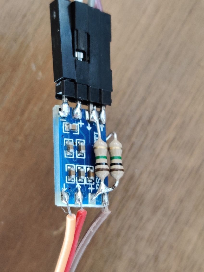
Now the easy part. I had a few MAX3232 modules which do the RS232 level shifting/inverting. On the Portfolio side I just need Ground, Tx and Rx. On the RC2014 side, Ground, 5v, Tx and Rx. Soldering was about as easy as things get, and it all looked good. Just to be safe, I decided to add an extra step and connect it to my FTDI adapter plugged in to the PC. A second later I dropped it as I felt burn my fingers!
Quickly unplugged everything and checked the soldering, the pin labels, and made sure I was 100% confident that everything looked fine. Plug it in again, touch the chip… Ouch! This was not good.
Time to bust out the FLIR thermal imaging camera. Wow! This thing gets up to 150’C (or 300’F) before I chicken out and pull the power.
Checking online and social media, people had reported problems with the cheap Chinese MAX232 modules. I had my doubts that the chips were genuine. However, some reports stated that the internal pull-up resistors are too weak, so without an input signal it is bouncing around all over the place and causing it to heat up. Others said that a resistor inline with the 5v power might fix it. Those ideas were certainly worth a try.
I can confirm, for my module at least, pull-up resistors made no difference. A resistor in series with the 5v meant that it didn’t get hot… but it didn’t work either. (although quite possibly the vital parts were already burned out?)
It was also pointed out that the chip is actually a MAX3232, which is a 3v3 chip. This would explain a lot! However, the datasheet says that it can work with Vcc from 3v – 5.5v. The TTL input can also be 5v even with a 3v3 Vcc. So, if it is a genuine chip, it _should_ still work
So I had to accept only a partial success, but mostly a failure on this one. The RC2014 worked at 9600 baud on Port B, and the Portfolio could talk at 9600 baud. It was just that they hadn’t talked to each other.
When I failed to complete the Retro Challenge in 2016 I finished by saying that the dog ate my homework. That sounded like a reasonable enough excuse.
This year any failure to complete is because The Riddler ate my schematic!
One of the first things I wanted to do was familiarise myself with what 2016-me did regarding the ZX81 module I designed for the RC2014. I have 3 PCBs here, and whilst they look great, they lack some info, such as the component values. So I opened up the schematic I created and discovered that all of the components have been replaced by ?? boxes!
To be fair, this isn’t the first time I have seen this situation. This was probably created in Kicad v4 or possibly earlier, and one thing which Kicad was terrible with back then was keeping track of component libraries whenever there was an upgrade. I am now using Kicad v8, so there have been a lot of upgrades.
I might be able to install a fresh copy of an old version and hope that has the right libraries and I can map them in to work with the schematic. I think that most of the components are resistors and capacitors though, so even if that worked, I wouldn’t have the values anyway.
I think it will actually be easier to convert the schematic to the v8 standard and manually change each of the parts to the resistor, capacitor or diode as approprite. I still won’t have the values, but the thing I do have is the original ZX81 schematic that this module was based on, so it should be a case of matching things up.
Mid-blog update
I looked back at the intro post that I made and noticed that the photo I reused from 2016 was a picture of the partially assembled module that was sitting on a schematic printout. The values can be seen too!
So that makes life easier!
Not only that, but another blog post from 2016 also has the full schematic (less component values) so that helps too!
The RC2014 has come along way since this module was conceived 8 years ago. I think some of the stuff that I had learned about the ZX81 back then had guided some of the decisions that I made later, which actually helps this a lot.
Firstly, the Backplane 8 and Backplane Pro both have the ability to add resistors on the data and address bus, as the ZX81 did. There is now an RC2014 keyboard which mimics the ZX81 or Spectrum layout and has the diodes onboard, so that makes things easier too. The Pageable ROM module supports 16k blocks, which will help if anything on the ZX81 needs to access the shadow ROM in 0x2000 – 0x3FFF. And, lastly, the 64k RAM module can be set to start at any address. With the ZX81 having RAM mapped from 0x4000 – 0x8000 this is perfect.
It has been a while since I entered Retro Challenge, but I think I remember what to do. It goes something along the lines of stating at the start of the month by saying that you are going to design a ZX81 module for the RC2014, and then at the end of the month report back in with minimal progress. Looking back, I seem pretty good at that. Retro Challenge 2016/1 started off like this and ended like this. Then later for Retro Challenge 2016/10 it looked like this.
I hope you will excuse me for using the same image I finished on 8 years ago, but, honestly nothing has changed. The ZX81 module is still in this state.
So, before we get to far ahead of ourselves, lets take a look at how we got to this point. My original goal was to recreate either a ZX Spectrum, ZX81, ZX80 or Jupiter Ace module for the RC2014. They are all fairly similar architecture, although the Jupiter Ace has weird dual port memory RAM. They all have a Z80 CPU, some ROM, some RAM and a clock, the same(ish) as theRC2014, so those parts of the schematic can all be ticked off. The ZX80 does everything else with conventional 74 series logic. The ZX81 is almost identical, except that 74 series logic is all smooshed in to a ULA. The Spectrum is similar except the ULA does more stuff (which can also be done with 74 series logic).
I ended up choosing the ZX81 as a good place to start because it is pretty much just a ULA chip with a little bit of support circuitry. The ULA is no longer manufactured, which will mean taking one from a working ZX81 to get this up and running. There are, however, modern FPGA replacements available, so I might well end up getting one of those to swap in at some point. So in January 2016 I translated the relevant parts of the ZX81 schematic in to KiCad and designed a module around that. I got some boards made, but that was as far as things got. Then later that year I soldered in 9 components.
To get started this year I need to do two things. Firstly, familiarise myself with the ZX81 circuit and the one I designed 8 years ago. I seem to remember being fairly confident it would work, but at this stage I have Schrodingers PCB. It both works and does not work simultaneously, needing a test to clarify the actual state. The second thing is that I need to check my stock of ZX81 and select a donor one that the ULA can be borrowed from. I probably want to make note of some of the pin voltages or signal traces before taking it out so I can check those when it is in the module.
There is a chance that I will end up waiting for parts, so the secondary part of my Retro Challenge challenge is to talk to my RC2014 with as many of my retro computers as possible. This may include but not be limited to;
Atari Portfolio
Cambridge Z88
Psion Organiser II
Psion Organiser 3a
Sinclair Spectrum (with Interface I)
Sinclair Spectrum 128
Sinclair Spectrum +2 or +3
Sinclair QL
Amstrad PPC640
Toshiba T1200
I think this will be limited to serial communication, and luckily I have a few MAX232 chips and boards here. I expect it will mainly be using the device as a serial terminal for the RC2014, but it would be nice to maybe send a Spectrum loading screen from the RC2014 to the Spectrum. It might sound trivial, but understanding how the serial ports work on those devices, and finding/writing software to use them could be the challenging part.
2024 marks the 10 year anniversary since I entered the Retro Challenge in… hmmm… let me see now… that’ll be… 2014! Yes, I remember it well, because Retro Challenge 2014 had a catchy hashtag on Twitter, something like #RC2014.
Well, the good folks behind Retro Challenge approached me and asked if I would consider donating a prize for this years event. There were no prizes back in my day, it was all about likes and subs, and inadvertently starting a new career back then. But, hey, I understand that people like prizes, so I said yes. I said I would like to offer an RC2014 Classic II kit to the winner of the RC2014 category
After thinking about it for a little while, I figured I could come up with something a little bit more special. But before I reveal what that is, and before you skip to the bottom of this post for a sneak peek, I wonder if I should explain what Retro Challenge is. Well, it is a challenge revolving retro computers. The challenge is self-set, and you can do pretty much whatever interests you if it involves a retro computer, and you blog about it to share your knowledge and inspire others. Maybe you want to right software for your old Dragon 32, or get that VIC20 cleaned up, recapped and retrobrited, or scan in the original PDP manuals and upload them to the Internet Archive.
Back in 2013 I had built a Z80 computer on a breadboard that ran BASIC. The challenge I set myself for Retro Challenge 2014 was to make my name appear in lights. More specifically I was going to write Z80 code to do it, using a Z80 computer which I also had to design. You can read more about it here https://rc2014.co.uk/653/retro-challenge-2014/
Part of the challenge was to get the PCBs designed and manufactured. I used OSHPark which meant I had 3 of each board. Luckily the designs worked and no serious modifications were needed (although a hammer was required to fit the header pins). You can read about the boards arriving here https://rc2014.co.uk/791/retro-challenge-pcbs-arrived-and-built/
Of the three sets of PCBs I had made, one set was used to build my original RC2014. Obviously. Another set was traded with John Fletcher for an original unpopulated Jupiter Ace PCB (See https://sowen.com/995/ace-adventures-on-jupiter/), and the feedback from that made me wonder if I should get some more made in case anybody else wanted to build their own RC2014.
So, what about the third set? It could be yours!
That’s right. In addition to the RC2014 Classic II kit, I will be giving away the final set of the original RC2014 PCBs to the lucky winner. Well, the original 32k RAM, Pageable ROM, Serial I/O and clock/reset module. The CPU module is a later one which the PCB manufacturer screwed up and didn’t put the silkscreen on the back! And I will throw in an original Digital I/O PCB too. As well as some stripboard.
Everything needed to complete the build is part of the Classic II kit. So when you receive your prize, you will need to decide if you want to build it as a Classic II, or go old school and make the most authentic RC2014 there is.
Not sure if I should put some legal disclaimer here or whatever. The winner will be chosen by the Retro Challenge organisers. I will post out the Classic II kit along with the original RC2014 PCBs mentioned above to the winner within a month of the winner being announced. This includes free international shipping if you are outside of the UK. No cash alternative is offered. Neither myself or the organisers of Retro Challenge can be held liable if you end up starting a new career based on your competition entry.
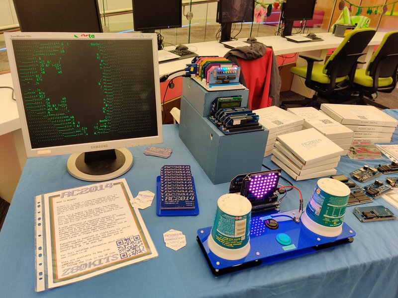
In July 2024 I was exhibiting at Liverpool Makefest again. This is a fantastic family friendly makers event that is open to the public for free. It has always been a great place to show off the various RC2014 kits as well as have something interactive that can keep people entertained.
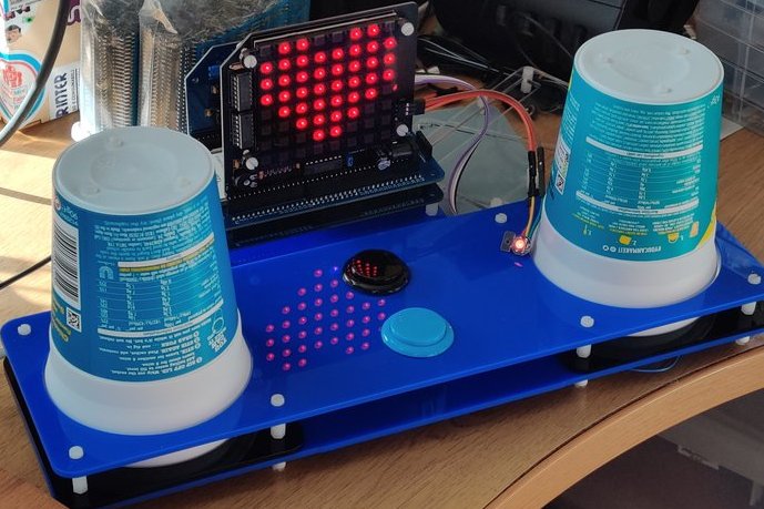
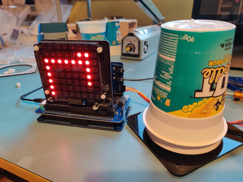
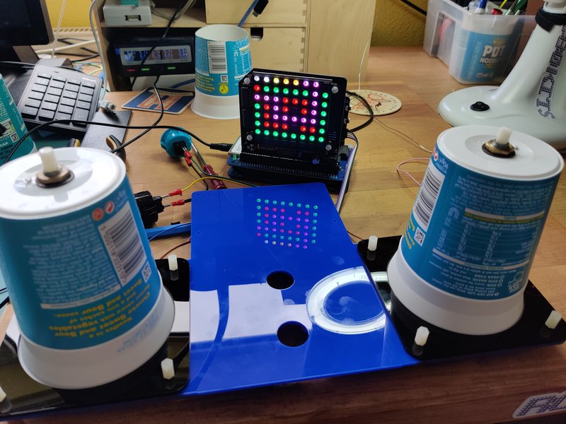
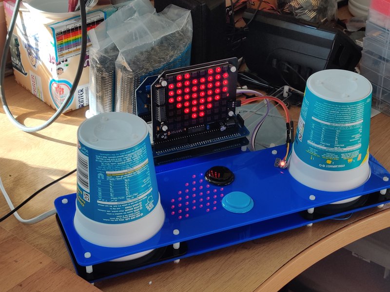
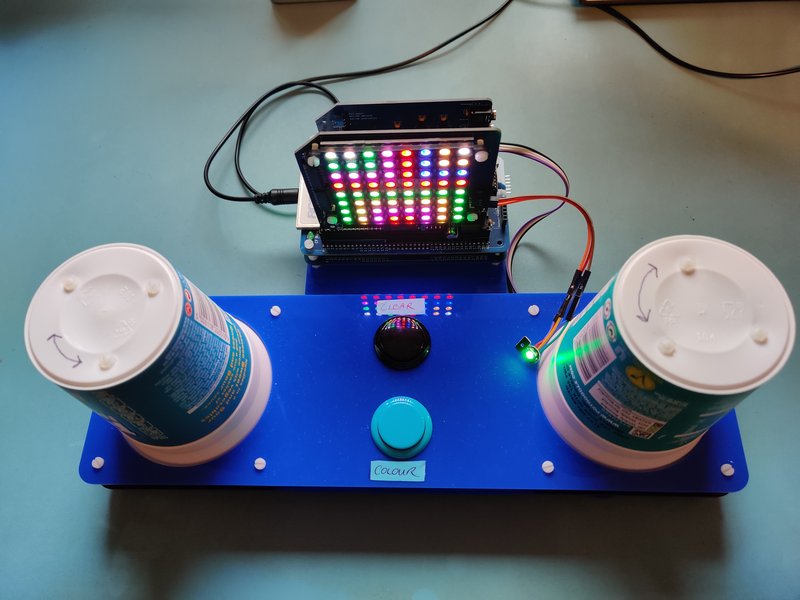
Normally I have a machine set up running Snake, but this year I was about to launch the Dual Paddle Analogue Module, so I wondered about making something with that. The idea of an Etch-a-sketch came up, and coupled with a NeoPixel Matrix Module I figured this would be a nice self contained demo unit.
I could handle the electronics and the physical build, but I reached out to Shiela at Peacock Media to see if she could help on the software side. As both the Dual Paddle Analogue Module and the NeoPixel Matrix Module were Shielas design she jumped at the idea. it was only 5 days before the event though, so we needed to move quick.
There were some important design considerations. Firstly, it had to be robust. One thing about the audience at Liverpool Makefest is there are quite a few kids and they are not always gentle with the exhibits. It also needs to be intuitive. If people need to read instructions, or things don’t give a satisfying output in the first few seconds they you have lost them. On top of that, it should really be self contained to the point where there is no need for a monitor or keyboard, and it just runs as soon as power is applied.
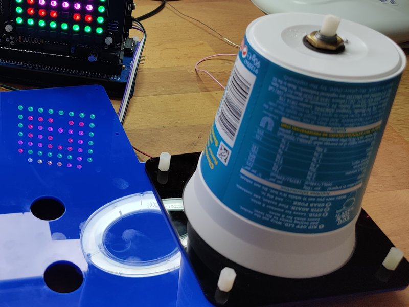
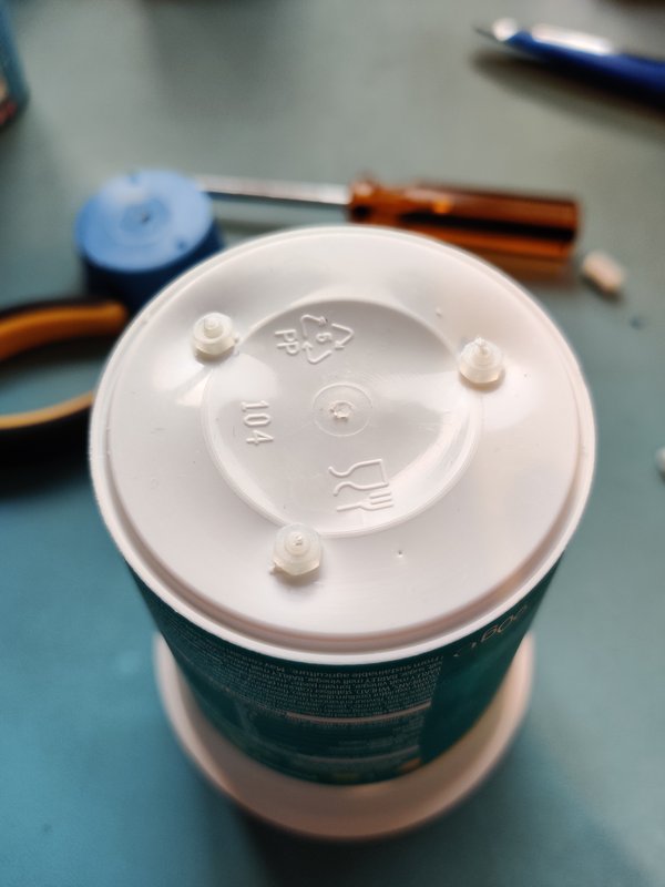
The first thing I needed to work out was the control mechanism. Two potentiometers, obviously, for X and Y, but how are they going to me mounted. I ran through some gamepad type prototypes but things weren’t quite feeling right. Then I noticed a couple of Pot Noodle pots sitting on my desk. These tapered plastic pots are great for pencil pots or other storage, and they stack really nicely. Two stacked together actually turn really nicely and feel good. But could a Pot Noodle pot house a pot? The Pot Noodle was launched at the same time as the Z80, so it seems like destiny, right?
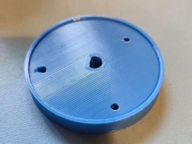
Off to the laser cutter to knock up a prototype. This consisted of a flat square plate with 3.5mm holes in the corners, and another matching plate that had a 100mm hole. This hole was slightly smaller than the brim of the pot, so when screwed down it holds the pot really really tightly to the base. With another pot on top it rotates really well. Putting 10mm standoffs and another pate with 100mm hole in it still allows it to rotate and it prevents the top pot from coming off.
fixing a 10k linear pot to the lower pot was easy enough. I used these lovely vintage RS pots that have a D-shaft
However, fixing the top pot to the shaft was a challenge. Making a D-hole in the top didn’t sound robust, so I decided to 3D print a couple of parameterised knobs in OpenSCAD. I could then glue these inside the top of top pot.
Dear reader, let me share one thing I now know about gluing PP (Polypropylene) plastic that the pots are made of PLA (polylactide) the 3D print it made of – you cannot! There isn’t a glue or solvent that will work. Trust me, I tried many many things.
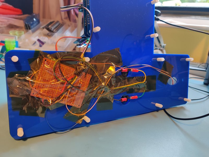
However, mechanical fasteners (M3 nuts and bolts) do work! The image above shows some holes drilled in the 3D part. Similar holes were drilled in the pots and they were bolted together. Rugged, child-proof and even repairable if needed!
This could now sit on the D-shaft of the pot, and kept from being removed by the top plate.
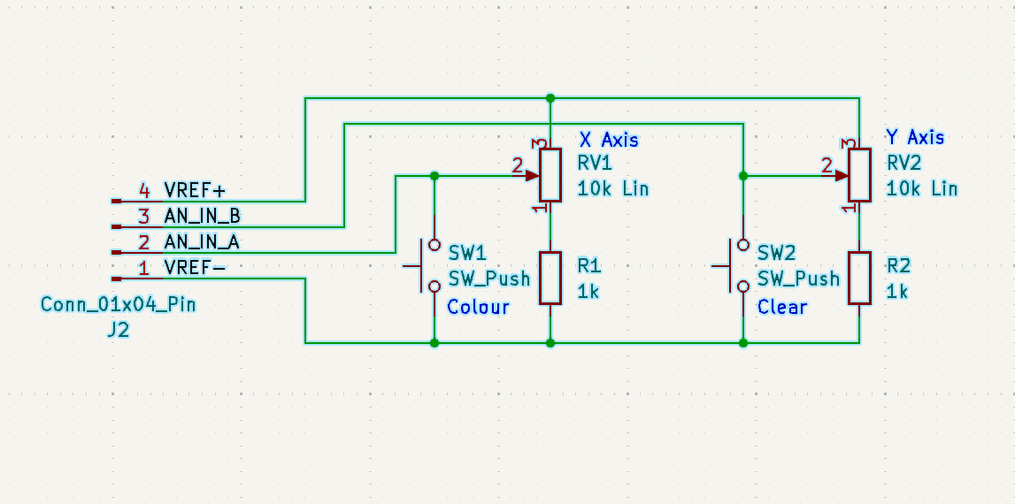
Next the question about additional controls. Whilst the original Etch-a-sketch was monochrome, the NeoPixel display didn’t have this limitation. There are a few ways to add a digital button to an RC2014, but when there is already an analogue module plugged in, it would be nice to use that.
To achieve two buttons of input, a 1k resistor was added to the negative side of the pot and a switch on the wiper going to ground. In normal use the 8 bit value from the variable resistor will only go down as low as 23, and as high as 255. When the switch is pushed the value is 0. So the software only needs to map approximately 25-255 to the 8×8 display, and anything less than 10 can be treated as a button press. With two pots, this allows 2 buttons, one for to cycle the colour, the other to clear the screen.
Note that it is tempting to put a 1k resistor and another switch going to the 5v line. This will give an extra two buttons, which would be great. However, if both buttons are pushed at the same time it will be shorting 5v and ground. This is a Bad Thing™ and certainly not something you want on a public facing exhibit. Even with a “do not push both buttons at the same time” sign!
A couple of arcade buttons worked great for this, although a label was put on as an afterthought as they weren’t quite as intuitive as hoped.
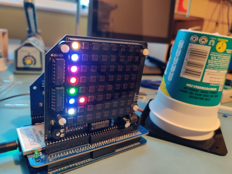
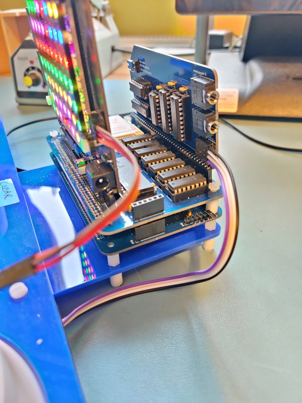
Shielas software worked great! Burning this on to ROM meant that it just ran on startup without any faffing at all. And with a t-shaped frame that housed the two pots, the buttons, and an RC2014 Mini with NeoPixel Module as well as the Dual Paddle Analogue Module it was a really nice self contained unit.
Things aren’t quite so neat underneath as the wiring for the pots and switches are all routed to a prototype board held together with Kapton tape. But nobody ever looks underneath, right?
How did it go? Great! As always, Liverpool Makefest was a great day out. The folks in Liverpool seemed to instinctively get it straight away. Some people spent a while creating their own Mona Lisa, and others tried teamwork with one person controlling the X axis and the other controlling the Y axis. Nothing broke down or needed restarting and it is all ready for the next event. If anything, the only failing was that it worked too well that nobody particularly asked how it was working, so I didn’t get to talk about the analogue module too much. But at least I got a blog post out of it :-)