Back in the earliest days of the RC2014, it came with a pre-programmed 27C512 64k ROM, with Microsoft BASIC on it in the first 8k, and it would work with 32k of RAM and a 68B50 ACIA. One set up, one ROM, life was simple!
As time has gone on, and more options have become available, other ROM images, such as Microsoft BASIC for 56k RAM, CP/M Monitor, RomWBW and Small Computer Monitor have been introduced. See this page for a brief overview of each option
Future possibilities, such as other UARTs, different CPUs or other variations will inevitably lead to more ROM images being needed. So, in order to keep track of what is programmed where, ROMs are now being shipped out with a label on them.
27C512 64k ROM
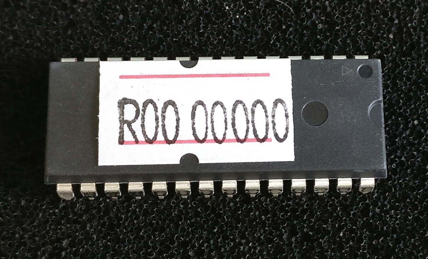
Every 64k ROM now has an 8 digit code on it. Each digit, from left to right, refers to an 8k bank from 0x0000 to 0xD000. This bank can be selected with the A13, A14, A15 jumpers;
| Address | A15 | A14 | A13 | ROM Label |
| 0000 | 0 | 0 | 0 | Xooooooo |
| 2000 | 0 | 0 | 1 | oXoooooo |
| 4000 | 0 | 1 | 0 | ooXooooo |
| 6000 | 0 | 1 | 1 | oooXoooo |
| 8000 | 1 | 0 | 0 | ooooXooo |
| A000 | 1 | 0 | 1 | oooooXoo |
| C000 | 1 | 1 | 0 | ooooooXo |
| E000 | 1 | 1 | 1 | oooooooX |
The value of the digit represents the ROM image that sits in that particular 8k bank. Currently, it will be one of the following;
0 – Empty bank, available for user to program
R – Microsoft BASIC, for 32k RAM, 68B50 ACIA, with origin 0x0000
K – Microsoft BASIC, for 56k RAM, 68B50 ACIA, with origin 0x0000
1 – CP/M Monitor, for pageable ROM, 64k RAM, 68B50 ACIA, CF Module at 0x10, with origin at 0x0000
2 – Microsoft BASIC, for 32k RAM, SIO/2, with origin 0x0000
4 – Microsoft BASIC, for 56k RAM, SIO/2, with origin 0x0000
6 – CP/M Monitor, for pageable ROM, 64k RAM, SIO/2, CF Module at 0x10, with origin at 0x0000
88 – Small Computer Monitor for pageable ROM, 64k RAM, SIO/2 or 68B50 ACIA, with Microsoft BASIC and CP/M boot options [Note that this is a 16k image, so Page Size needs to be set to 16k and only A14 and A15 jumpers to select]
9 – Small Computer Monitor for any ROM, any RAM, any UART
Mini II
To further complicate things, the Mini II ships with an ST39SF010 – a 128k Flash RAM which is divided up in to 8 x 16k pages, or 16 x 8k pages, or some combination of those. There are different options for BASIC, SCM CP/M and also FORTH.
Chips are labelled as “M2 1.2”
ST39SF040 512k RomWBW 2.9.1
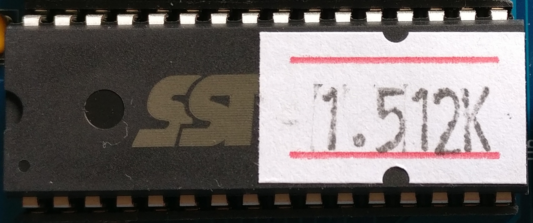
Version 2.9.1 of RomWBW needed to be compiled differently, based on what peripherals were to be supported. To indicate which peripherals the ROM had support for, the designation of x.512K is used, where x is the software designation.
1.512k – RomWBW RC_Std.ROM 2.9.0
2.512k – RomWBW RC_Std.ROM 2.9.0 With PPIDE
3.512k – RomWBW RC_Std.ROM 2.9.0 With RTC
4.512k – RomWBW RC_Std.ROM 2.9.0 With PPIDE and RTC
5.512k – RomWBW RC_Std.ROM 2.9.0 With WDC Floppy
6.512k – RomWBW RC_Std.ROM 2.9.0 With WDC Floppy and PPIDE
7.512k – RomWBW RC_Std.ROM 2.9.0 With WDC Floppy and RTC
8.512k – RomWBW RC_Std.ROM 2.9.0 With WDC Floppy, PPIDE and RTC
ST39SF040 512k RomWBW 3.0 onwards
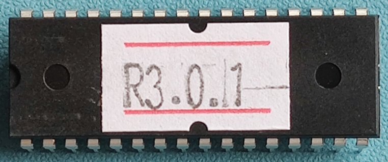
Since the release of RomWBW 3.0.0, peripherals are automatically detected, so there is no need for different builds. Therefore the label will just indicate the revision programmed. At the time of writing, as indicated above, the latest stable release is 3.0.2
As more ROM images are added, this list will be updated.
Standard factory ROM images can be downloaded from Github https://github.com/RC2014Z80/RC2014/tree/master/ROMs/Factory
Note that despite having total control over which designation I want to use for whichever ROM image and where that is located on the ROM – I still managed to pick a combination that my label gun was unable to do! So some people will have a label that starts with an interlocking “n” and “u” character, which is the closest I could do to represent a “2”. If this is the case, your “¬4006000” is actually “24006000”. In order to get around this, I have now bought an extra 2 label guns, which have been dismantled to allow the belts to be swapped around, and reassembled. Normally reassembly of label guns is only possible by a highly skilled and qualified octupus, so I don’t recommend anybody tries doing this themselves!