One of the things I am keen to promote about the RC2014 is that designing your own modules is very simple and straightforward. The standard bus layout gives access to all of the basic signals that you are likely to need and the enhanced, or v2.0 layout builds on this with access to extra lines. PCBs can, of course, be whatever shape and size you want, but you may have noticed that since around April 2016 I have settled on a standard shape for all new modules.
In this post, I want to discuss the past, present and future of the RC2014 bus, the physical modules, and what you might want to bare in mind when designing your own modules.
Mechanical Layout
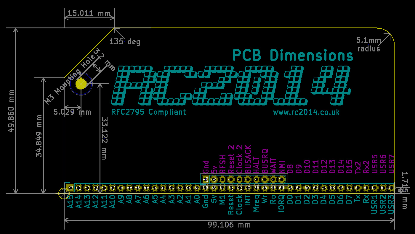
Firstly, to dispel a few myths about the shape of this; It was not designed to mimic an SD Card, a New Document icon or even an Apple II expansion card. The shape was actually inspired by the Hollerith, or IBM punched cards with the cut off corner being an easy way to identify which end Pin 1 is.
The default size, 99.1mm x 49.9mm was chosen to fit within a standard 10cm x 5cm PCB manufacturing size, whilst also being within the 100mm limit of the free Eagle licence. (Personally, I use and recommend KiCad, which does not have such limitations).
A drawback of the length is that there is only room for a 39 pin header. To comfortable fit a standard 40 pin header it would need to be 104mm. Therefore, the length is nominal and can be adjusted, either longer to accommodate the extra pin, or shorter to reduce PCB cost if necessary.
Height is also nominal – although a suggested ‘low profile’ height of 38.1mm could be used, which will allow for a small angled cut off to indicate pin 1 and also leave room for the mounting hole.
The 45° corner cut off not only signifies the orientation of the module, but would allow for a case to be designed to take advantage of this.
The mounting hole can also be used in case design to anchor all modules in place if necessary.
A KiCad template can be downloaded here (delete the .txt extension and rename it according to your KiCad project)
Bus layout
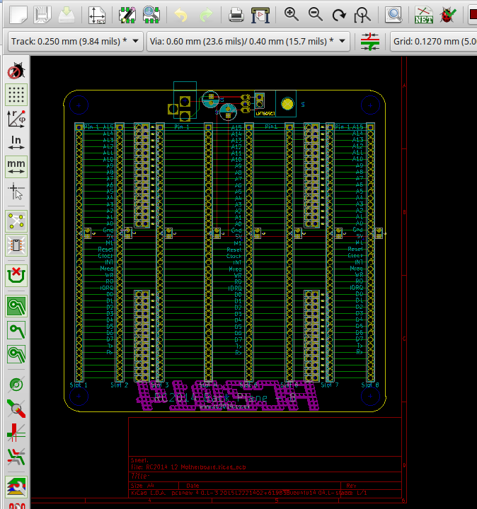
When the idea of the RC2014 was conceived, the goal was to get a Z80 based computer running on a backplane as simply as possible. Some signals that were not required in the basic design, such as BUSRQ, were not bought out on to the backplane and were simply terminated on the CPU module. As the RC2014 has developed, however, some of these signals are needed to support more advanced modules such as the SD Memory Dump Module.
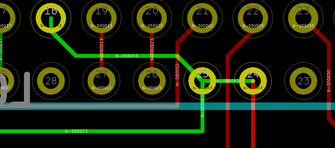
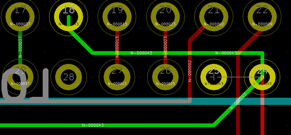
The challenge has been to expand the bus to allow for this, whilst keeping things compatible with older modules and backplanes. The solution is to add an ‘enhanced bus’ – a partial secondary line of pins above the original (on the module) and to the left of the original (on the backplane). Standard right-angle header pins can be used for the original parts and double right-angle header pins used where the enhanced bus is needed.
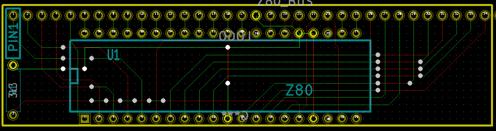
Standard Bus
The original RC2014 only needed 34 pins to operate, with an extra 2 if the serial module is to talk to other modules. This leaves 4 pins of the 40 pin header which users are free to use for whatever they want – however, be aware that using pin 40 will take the module over 100mm (see mechanical layout above)
| Pin | Label | Description | Note |
| 1-16 | A15 – A0 | Address lines for up to 64k of addressable memory | |
| 17 | Gnd | 0v power supply | |
| 18 | 5v | 5v power supply | |
| 19 | M1 | M1 control line from CPU | Active Low |
| 20 | Reset | Reset line for CPU and optionally other modules | Active Low |
| 21 | Clock | Main CPU clock signal and optionally other modules | |
| 22 | INT | Interupt | Active Low |
| 23 | MREQ | Memory Request | Active Low |
| 24 | WR | Write | Active Low |
| 25 | Rd | Read | Active Low |
| 26 | IORQ | I/O Request | Active Low |
| 27 – 34 | D0 -D7 | 8 data lines | |
| 35 | Tx | Serial transmit | |
| 36 | Rx | Serial receive | |
| 37 – 39 | USR1-3 | 3 spare pins for user functions | |
| 40 | USR4 | 4th spare pin. Suggest it is not used | Avoid |
Enhanced Bus
The enhanced, or v2.0 bus, adds to the standard bus to allow for backwards compatibility whilst giving access to other control lines not available on the original bus. This is intended to be an optional bus, only used if it is required. However, if it is used, the 10 pins in the center should be the minimum. Having additional clock, reset, Tx and Rx lines opens the RC2014 up to more advanced peripherals and the extra 8 data lines would be required if a 16 bit CPU was used.
| Pin | Label | Description | Note |
| 1-16 | Not used | ||
| 17 | Gnd | 0v power supply | |
| 18 | 5v | 5v power supply | |
| 19 | RFSH | M1 control line from CPU | Active Low |
| 20 | Reset2/Page | Secondary reset or page line for other modules | Active Low |
| 21 | Clock2 | Secondary clock line for other modules | |
| 22 | BUSACK | Bus Acknowledge | Active Low |
| 23 | HALT | Halt | Active Low |
| 24 | BUSRQ | Bus Request | Active Low |
| 25 | WAIT | Wait | Active Low |
| 26 | NMI | Non-maskable Interupt | Active Low |
| 27 – 34 | D8 -D15 | Additional 8 data lines (for 16bit CPU) | |
| 35 | Tx2 | Secondary serial transmit | |
| 36 | Rx2 | Secondary serial receive | |
| 37 – 39 | USR5-7 | 3 spare pins for user functions | |
| 40 | USR8 | 4th spare pin. Suggest it is not used | Avoid |
Making your own modules – Designed for RC2014
If you wish to design your own modules, you are, of course, free to use whatever shape, size or pin arrangement you wish. However, keeping to the above guidelines should give your modules compatibility with other RC2014 modules. If your module may be of use to other RC2014 owners, please consider sharing your design or selling them yourself. I’m happy to help you with this and to spread the word. Note that “RC2014” is a registered trademark, so you are not allowed to call your module “RC2014 [thingy] Module” or use the RC2014 logo. However, feel free to mark your modules as “Designed for RC2014”
If you need clarification on anything here, please feel free to contact me directly using the Contact Me link or start a thread on the RC2014-Z80 Google Group.