Ok, with 5 days of October already gone, I know it’s cutting things a bit fine for putting my entry in for this seasons Retro Challenge – particularly as it started 5 days ago… but, better late than never, right?
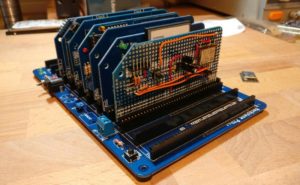
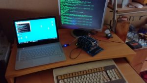
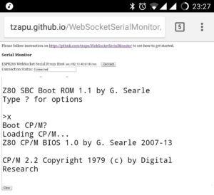
So, what have I planned to do that is both retro and challenging? Simple, I’m going to play games! More specifically, I’m going to play Zork, on a CP/M enabled RC2014 that is connected to the internet so it can be streamed live to an audience of anybody that cares to watch me get eaten by a grue.
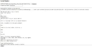
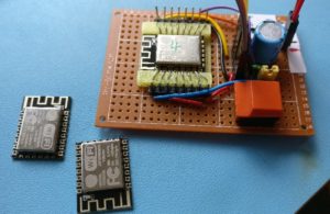
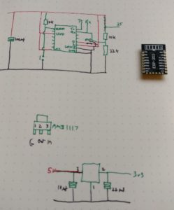
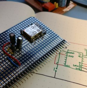
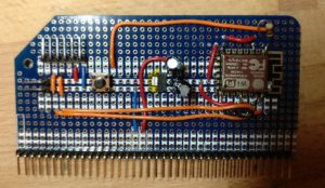
The first challenge is going to be hooking up the RC2014 to the internet, such that it can stream text. Kind of like Twitch, but in ASCII. Luckily, I’ve got a bunch of ESP8266 modules that have been sitting in a drawer, and I think these are likely to be ideal for converting serial data in to web pages. I should be able to hook up something on breadboard, and find a bit of code that does the job – although it would be nice if I can get some real PCBs made up for the job. With just over 3 weeks to go, though, that might be pushing it timewise.
Then there is the challenge of Zork itself. I often use it as a test game to show people what the RC2014 can do, however, I’ve never done more than a bit of random North, North, East, Look, Get Lamp etc. I’ve never really played many text adventures either, so this will be a big learning experience for me. I can’t promise that I won’t use the odd cheat/clue here and there, but if there are actually people watching along online, I’ll happily take suggestions over Twitter. If things happen to go really well, and I complete it in good time, then I will add Adventure as a stretch goal.
Since the first days of selling RC2014 kits, I’ve been cutting resistors off of bandoleers. Depending on the kit, they might be singular, or in groups of 3, 4, 5 or 8. To cut off a single resistor with a pair of scissors is very quick and simple. However, doing it time and time and time again, or having to count to cut them in to blocks of 5 can get time consuming and monotonous. Of course, there are industrial machines to automate these, but they cost a lot of money and are designed for doing thousands per day.
Then there are more hobby level machines, like this one from Oomlout. If I had a laser cutter, some servos, an Arduino and a few other bits, I could make one of these. So, when I purchased a laser cutter recently, building one of these was on my to-do list.
At some point, the redundancy became obvious. Why use a laser cutter to make a cutting machine – when the laser cutter is, itself, a cutter! So, 5 minutes with InkScape and I had a basic template ready to test
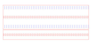
The template consists of 2 parts. The first, larger piece goes on the bed of the laser cutter. A strip of resistors is decanted on to the firsts part so that the resistors themselves sit in the holes running down the middle
The second half of the template then clamps the resistors in place and is held down with magnets (Note that the following photo was taken after they were cut!).
The laser cutter then cuts the tape! Depending on the template, this could be in groups of 1, 2, 3, 4, 5, 8 resistors.
And voila! Precision laser cut resistors!
The dxf file for this is available to download on Thingiverse so you can laser cut your own resistors.
This is the first iteration of this, and it works surprisingly well. Set up time isn’t too long, but if you only need a few resistors cut off, you’re better off doing them the old fashioned way with scissors. But for running off a batch of a couple of hundred or more, it’s certainly quicker and easier.
The lower part of the template will get repeatedly cut on the intersection of the resistor tape, and sooner or later this will need replacing. When that happens, I’m going to replace it with a much longer version, so I can do a lot more in one go. I’m also wondering about having a few tapes in parallel for even more speed – but this might be at the risk of mixing up different value resistors.
So, the next time you get a RC2014 kit, just take a moment to marvel at the precision at which your resistors have been trimmed off of the tape!
Having the ability to isolate some slots on the Backplane 8 can be very handy at times, and putting some protection in between modules can be very worthwhile. However, if you want to connect the outer slots, then soldering little links can be fiddly and time consuming.
Thankfully, there’s a quick and easy way to do it.
The photos are probably self explanatory, but get a length of 300-400mm of stripped solid core wire and solder it through one hole to hold the end in place. Then lace it all the way down, going horizontally on the top of the board and diagonally underneath. Don’t worry if it’s not too neat underneath. Solder each joint (I find it easiest from the top before all the sockets are in place, or from underneath if they are already fitted). Then simply cut all the diagonal links off of the underside. Job done!
Back in the earliest days of the RC2014, it came with a pre-programmed 27C512 64k ROM, with Microsoft BASIC on it in the first 8k, and it would work with 32k of RAM and a 68B50 ACIA. One set up, one ROM, life was simple!
As time has gone on, and more options have become available, other ROM images, such as Microsoft BASIC for 56k RAM, CP/M Monitor, RomWBW and Small Computer Monitor have been introduced. See this page for a brief overview of each option
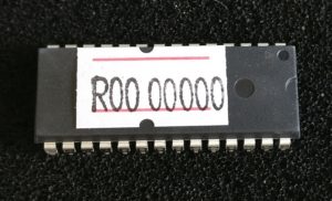
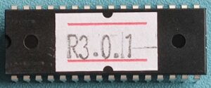
Future possibilities, such as other UARTs, different CPUs or other variations will inevitably lead to more ROM images being needed. So, in order to keep track of what is programmed where, ROMs are now being shipped out with a label on them.
27C512 64k ROM
Every 64k ROM now has an 8 digit code on it. Each digit, from left to right, refers to an 8k bank from 0x0000 to 0xD000. This bank can be selected with the A13, A14, A15 jumpers;
Address
A15
A14
A13
ROM Label
0000
0
0
0
Xooooooo
2000
0
0
1
oXoooooo
4000
0
1
0
ooXooooo
6000
0
1
1
oooXoooo
8000
1
0
0
ooooXooo
A000
1
0
1
oooooXoo
C000
1
1
0
ooooooXo
E000
1
1
1
oooooooX
The value of the digit represents the ROM image that sits in that particular 8k bank. Currently, it will be one of the following;
0 – Empty bank, available for user to program
R – Microsoft BASIC, for 32k RAM, 68B50 ACIA, with origin 0x0000
K – Microsoft BASIC, for 56k RAM, 68B50 ACIA, with origin 0x0000
1 – CP/M Monitor, for pageable ROM, 64k RAM, 68B50 ACIA, CF Module at 0x10, with origin at 0x0000
2 – Microsoft BASIC, for 32k RAM, SIO/2, with origin 0x0000
4 – Microsoft BASIC, for 56k RAM, SIO/2, with origin 0x0000
6 – CP/M Monitor, for pageable ROM, 64k RAM, SIO/2, CF Module at 0x10, with origin at 0x0000
88 – Small Computer Monitor for pageable ROM, 64k RAM, SIO/2 or 68B50 ACIA, with Microsoft BASIC and CP/M boot options [Note that this is a 16k image, so Page Size needs to be set to 16k and only A14 and A15 jumpers to select]
9 – Small Computer Monitor for any ROM, any RAM, any UART
Mini II
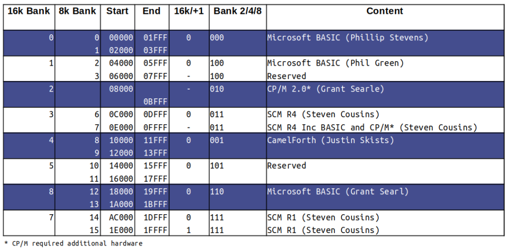
To further complicate things, the Mini II ships with an ST39SF010 – a 128k Flash RAM which is divided up in to 8 x 16k pages, or 16 x 8k pages, or some combination of those. There are different options for BASIC, SCM CP/M and also FORTH.
Chips are labelled as “M2 1.2”
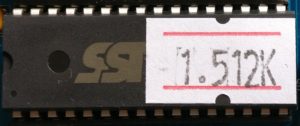
ST39SF040 512k RomWBW 2.9.1
Version 2.9.1 of RomWBW needed to be compiled differently, based on what peripherals were to be supported. To indicate which peripherals the ROM had support for, the designation of x.512K is used, where x is the software designation.
1.512k – RomWBW RC_Std.ROM 2.9.0
2.512k – RomWBW RC_Std.ROM 2.9.0 With PPIDE
3.512k – RomWBW RC_Std.ROM 2.9.0 With RTC
4.512k – RomWBW RC_Std.ROM 2.9.0 With PPIDE and RTC
5.512k – RomWBW RC_Std.ROM 2.9.0 With WDC Floppy
6.512k – RomWBW RC_Std.ROM 2.9.0 With WDC Floppy and PPIDE
7.512k – RomWBW RC_Std.ROM 2.9.0 With WDC Floppy and RTC
8.512k – RomWBW RC_Std.ROM 2.9.0 With WDC Floppy, PPIDE and RTC
ST39SF040 512k RomWBW 3.0 onwards
Since the release of RomWBW 3.0.0, peripherals are automatically detected, so there is no need for different builds. Therefore the label will just indicate the revision programmed. At the time of writing, as indicated above, the latest stable release is 3.0.2
As more ROM images are added, this list will be updated.
Note that despite having total control over which designation I want to use for whichever ROM image and where that is located on the ROM – I still managed to pick a combination that my label gun was unable to do! So some people will have a label that starts with an interlocking “n” and “u” character, which is the closest I could do to represent a “2”. If this is the case, your “¬4006000” is actually “24006000”. In order to get around this, I have now bought an extra 2 label guns, which have been dismantled to allow the belts to be swapped around, and reassembled. Normally reassembly of label guns is only possible by a highly skilled and qualified octupus, so I don’t recommend anybody tries doing this themselves!
The RC2014 currently uses a very simple, although inefficient method of addressing peripherals. Most of the expansion modules feature a 74HCT138 used to provide up to 8 enable lines from 3 address signals. For the purposes of this document, I will mainly refer to the Digital I/O Module, but the principals apply to all modules with a 74HCT138 (generally referred to simply as ‘138)
It is worth noting that the Z80 CPU can address up to 256 Input or 256 output addresses. These are selected by the first 8 address lines (A0 – A7), IORQ going low and either WR or RD going low.
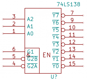
The ’138 has 3 enable pins, G1, G2B, G2A, all of which need to be true (G1 needs to be high, and both G2B and G2A need to be low) for the ‘138 to be enabled. When it is enabled, the 3 address lines, A0, A1, A2 are read. These 3 addresses have 8 possible combinations (000, 001, 010, 011, 100, 101, 110, 111), which will activate one of the 8 outputs Y0 to Y7.
In the Digital I/O Module, the ‘138 is activated when M1 is high, IORQ is low and A7 is low. This corresponds to any port from 0 to 127 (IORQ being low indicates the address bus represents port, and A7 being low indicates the address bus is lower than 127). [Side note – Serial I/O Module uses addresses 128 and 129, which are indicated by A7 being high].
The Z80 address pins A0 and A1, along with WR are connected to the address pins A0, A1, A2 on the ‘138. This gives 4 addresses (00, 01, 10, 11) with the write bit high, and 4 with it low.
In normal use, the ports are addressed as 0 (In 0 or Out 0) on the Digital I/O Module. (Or port 0, 1, 2 on the Digital Input module, for example). However, any address that has A0, A1 and A7 low will work; 0—–00. So echoes of this will appear on 4, 8, 12… 124. So, whilst this works, and is fine for a small system without much I/O requirements, it quickly becomes inefficient as you need more ports. In particular, it will clash with the Compact Flash Storage Module, which can have an impact on running CP/M.
In an ideal world, every peripheral should have a unique address, and with a lot of digital logic, this is certainly possible to do. However, it will add both complexity and cost as well as needing more board space.
The easy solution, however, involves just 6 diodes and a resistor. By connecting address lines A2 – A7 to the anode of each diode and the cathode of each diode to the G2A enable pin on the ‘138, any address above 00000011 will prevent the ‘138 from being enabled. Effectively all the diodes are acting as a very simple OR gate. A 10k resistor will bias the output low.
So with this set up, it will give just 4 unique addresses; 00000000, 00000001, 00000010, 00000011 (ie 0, 1, 2, 3) which for the Digital I/O Module, or the Digital Input or Digital Output is ideal.
Other addresses can be selected by changing which address pin the diodes are connected to. So, for example, if A1 was connected to a diode instead of A3, and A3 went to the ‘138, the addresses would be 00000000, 00000001, 00001000, 00001001 (ie 0, 1, 8, 9). Whilst it cuts down on the echoes at higher addresses, it’s still not perfect – but much better and still very cheap with minimal extra board space needed.
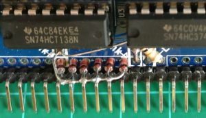
The Digital I/O Module has now been updated to reflect this change. As PCB stocks run low on other modules, they too will have similar updates. If you already have a non-diode selectable module, and wish to implement this, it is actually very simple to do as shown below.
With the right software, hardware and settings, getting CP/M running on a RC2014 is very easy. This post is a guide to doing just that. It assumes you are already familiar with the RC2014 and have built and tested your RC2014 running BASIC.
Both the Pageable ROM Module and the Compact Flash Module are available with the CP/M Monitor pre-programmed on to ROM at 0x8000.
The Compact Flash Module is also available with a pre-programmed 128mb compact flash card which contains CP/M as well as the essential software required to get you up and running
Settings
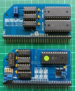
The 64k RAM Module needs to be set to full 64k (ie start address at 0x0000) and in pageable mode. For this, all 4 jumpers need to be set to the right hand settings as shown below. If you soldered a link where indicated by the silkscreen, this needs to be remove as this is the page pin
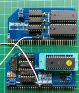
The Pageable ROM Module needs to be set for an 8k page and starting at 0x8000. See photos below for details.
The Page Pin from the ROM needs to be connected to the Page Pin on the RAM. If you have the Backplane Pro and have installed the double header pins supplied with that then nothing further needs to be done. If you are using a Backplane 8, however, you will need to add a jumper cable between the 4th pins on the 10 pin Enhanced Bus header. See the photos below to illustrate either scenario
Then it is simply a case of installing all the modules (if using Backplane 8 ensure you have links between slot 2&3 or 6&7 so you can use the outer slots), connecting FTDI cable or monitor & keyboard if you are using the Pi Zero Terminal, inserting the compact flash card and applying power.
[On power up, a small bootloader will copy itself and a modified CP/M console from 0x0000 (ROM) up to 0xA000 (RAM), then page out the ROM and page in the lower 32k RAM, then copy Grant Searles CP/M Monitor (as modified by Mitch Lalovie and tweaked by me) back to 0x0000 (RAM) and run the monitor from there]
You will be greeted by a “Press [space] to activate console” message, and after pressing space you will be in to the monitor.
(Note that the B option for BASIC will not work with this hardware set up. If you want to use BASIC, either set the A15 Page Selection jumper to 0, or download a copy of mbasic to CP/M)
Press X followed by Y and it will boot CP/M from the compact flash card and you will be at the A> prompt.
The compact flash card is pre-formatted with 16 drives from A: to P: The A: drive has DOWNLOAD.COM which is needed to transfer files on to the CF card. Drive C: has CP/M utilities such as TYPE.COM ED.COM, STAT.COM etc.
To copy files and programs on to the CF card you will need to connect to your RC2014 over a FTDI cable, and either use Grant Searles Windows File Packager or manually package the files with a text editor. When copied over the FTDI connection it will initiate A:DOWNLOAD.COM which will then take the file and put it on to the current selected drive. Note that the flow control on the 68B50 is minimal with this setup, so a 1ms delay between characters is suggested to give consistently successful results.
After that, I highly recommend using a torch otherwise you will almost certainly end up being eaten by a Grue
If you are planning on installing a module that makes use of the additional signals available on the Enhanced Bus with a Backplane Pro, then you will need to use a double row right angle header on the module.
Unfortunately, the profile of single and double row headers are quite different, and they cannot be mixed and matched on the same module.
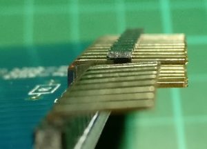
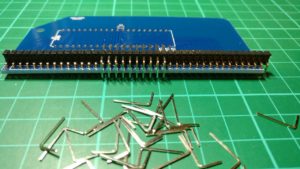
Removing the excess pins from a double row header is quite quick and simple, although if you mess up you could end up with pins out of alignment, and nobody wants that! However, there is a neat little trick that makes things even easier.
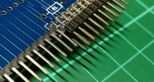
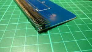
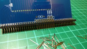
Start by putting the double row header on the module PCB backwards, so that the short pins all go through the holes. (Don’t solder them!). Instead of using your module PCB then anything such as Veroboard could be used, just ensure that only one row (the short pins) go thought. This will ensure that they stay in perfect alignment.
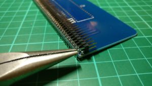
Then, with a pair of needlenose pliers, start to remove the long pins, beginning on the right hand edge
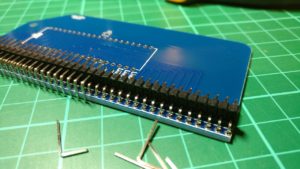
They should come out quite smoothly, although you might need to give some a little twist to loosen them up.
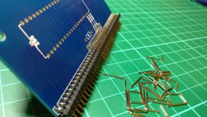
Keep on going until there are 16 pins removed.
Most modules have 10 Enhnaced Bus pins, so skip over 10 pins before removing the rest. (Note that because the pins are upside down, you can’t use the marking on the module as a guide as this is of-centre)
Of course, if your module has more than 10 Enhanced Bus pins, skip over this amount instead.
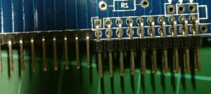
Remove the pins and put the header in the right way up. It should all line up, and you will have one pin (pin 40) to remove at the very end.
From the very earliest days of the RC2014, back when the whole thing was a bunch of wires and chips on a breadboard and before the RC2014 even had a name I knew that it needed some kind of storage. The obvious solution to me was via SD card. I had already made a simple PS2 keyboard and 4 line LCD display interface from an Atmel ATMEGA328, and it was easy enough to add an SD card interface. The ‘328 was connected to the yet to be named RC2014 via serial, so anything I could type on the keyboard could be passed through to the RC2014. Likewise, the contents of a text file on the SD card could also be put on the serial port. Intercepting keystrokes like F1 would send the text file 1.bas to the RC2014.
It kind of worked, but was clunky at best. The text files had to be created on a PC as there was no way to save anything – although I thought about monitoring the keyboard for SAVE to be typed which would be replaced by LIST and the stream coming back would be saved to SD. But that was even more clunky and hacky.
Once the RC2014 appeared in PCB form, I returned to the idea of an SD card storage device. This time it was to load raw machine code from SD to RAM – again, via an ATMEGA328 but this time connected via a Z80 port (Essentially, the same circuit as the Digital I/O Module)
The idea here would be a simple bootloader ROM would run on the RC2014. This would set one of the bits of port 0 high so the ‘328 would know to load the first byte from a file on the SD card on to the data bus. Once the Z80 had loaded this in to RAM it would toggle the bit and the next byte would be read until the whole file was loaded.
Although this worked, it wasn’t a solution I was particularly happy with. The main reason was that it had very limited functionality and relied on a custom ROM image.
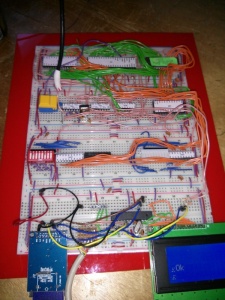
What I wanted was a way to fill the RAM without worrying about what’s in the ROM (or even having a ROM), and bypassing the Z80. An old idea that I had for making an EPROM burner was recycled in the form of this prototype;
This used a couple of 74LS393 counters connected to the address bus via 74LS245 to count from 0 to 65535 (ie the whole Z80 memory address space). A bus request (BUSRQ) from the ‘328 asked the Z80 to disconnect itself from the bus. When this is acknowledged (BUSACK) the ‘245s have control of the bus and can increment the address from a pulse from the ‘328. The prototype proved the concept worked, so time to spin up a simple board to take things further.
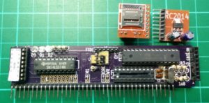
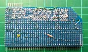
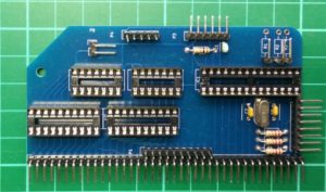
The first spin of the board was focused on the Z80 interface with the SD pins and any spare GPIO pins from the ‘328 bought out to headers. I still hadn’t decided yet how the SD card would actually be fitted. Every SD card socket I could find was surface mount, and if this was to be made in to a kit, I wanted to avoid surface mount components if possible.
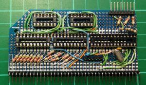
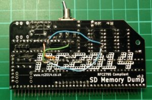
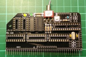
The next spin of the board refined more of the control circuitry. The spare GPIO pins had been connected to switches, LEDs and some of the bus lines. Not everything quite worked as planned, as the subtle bodge wires allude to. In hindsight, using black solder resist for a prototype board wasn’t such a great idea either. However, I got it to work and was able to get the firmware on the ‘328 doing what I wanted it to do.
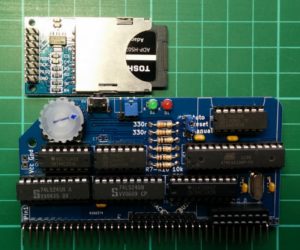
I had been using a cheap Chinese SD module to connect the ‘328 to an SD card, and these actually work very well as well as being a kind of standard, so to get around the surface mount issue, I decided to use the whole module in the finished product. Oh, and as you can see, there really isn’t much spare PCB space for an SD card socket either!
With a bit of swapping around, I managed to free up an analog GPIO pin that I could connect to a potentiometer. This works as a crude file selector. The initial firmware I wrote for the ‘328 works, and loads an image from SD card in to RAM, or dumps the whole contents of memory in to a file on the SD card. Scott Lawrence has updated this to give access to different file images and protects these against accidental overwriting.
So far, this is the best SD card storage for the RC2014 that I’ve made. I wanted to share this though to give you an idea of how a new module is created, from conception, through prototypes and to final product.
One of the things I am keen to promote about the RC2014 is that designing your own modules is very simple and straightforward. The standard bus layout gives access to all of the basic signals that you are likely to need and the enhanced, or v2.0 layout builds on this with access to extra lines. PCBs can, of course, be whatever shape and size you want, but you may have noticed that since around April 2016 I have settled on a standard shape for all new modules.
In this post, I want to discuss the past, present and future of the RC2014 bus, the physical modules, and what you might want to bare in mind when designing your own modules.
Mechanical Layout
Firstly, to dispel a few myths about the shape of this; It was not designed to mimic an SD Card, a New Document icon or even an Apple II expansion card. The shape was actually inspired by the Hollerith, or IBM punched cards with the cut off corner being an easy way to identify which end Pin 1 is.
The default size, 99.1mm x 49.9mm was chosen to fit within a standard 10cm x 5cm PCB manufacturing size, whilst also being within the 100mm limit of the free Eagle licence. (Personally, I use and recommend KiCad, which does not have such limitations).
A drawback of the length is that there is only room for a 39 pin header. To comfortable fit a standard 40 pin header it would need to be 104mm. Therefore, the length is nominal and can be adjusted, either longer to accommodate the extra pin, or shorter to reduce PCB cost if necessary.
Height is also nominal – although a suggested ‘low profile’ height of 38.1mm could be used, which will allow for a small angled cut off to indicate pin 1 and also leave room for the mounting hole.
The 45° corner cut off not only signifies the orientation of the module, but would allow for a case to be designed to take advantage of this.
The mounting hole can also be used in case design to anchor all modules in place if necessary.
A KiCad template can be downloaded here (delete the .txt extension and rename it according to your KiCad project)
Bus layout
When the idea of the RC2014 was conceived, the goal was to get a Z80 based computer running on a backplane as simply as possible. Some signals that were not required in the basic design, such as BUSRQ, were not bought out on to the backplane and were simply terminated on the CPU module. As the RC2014 has developed, however, some of these signals are needed to support more advanced modules such as the SD Memory Dump Module.
The challenge has been to expand the bus to allow for this, whilst keeping things compatible with older modules and backplanes. The solution is to add an ‘enhanced bus’ – a partial secondary line of pins above the original (on the module) and to the left of the original (on the backplane). Standard right-angle header pins can be used for the original parts and double right-angle header pins used where the enhanced bus is needed.
Standard Bus
The original RC2014 only needed 34 pins to operate, with an extra 2 if the serial module is to talk to other modules. This leaves 4 pins of the 40 pin header which users are free to use for whatever they want – however, be aware that using pin 40 will take the module over 100mm (see mechanical layout above)
Pin
Label
Description
Note
1-16
A15 – A0
Address lines for up to 64k of addressable memory
17
Gnd
0v power supply
18
5v
5v power supply
19
M1
M1 control line from CPU
Active Low
20
Reset
Reset line for CPU and optionally other modules
Active Low
21
Clock
Main CPU clock signal and optionally other modules
22
INT
Interupt
Active Low
23
MREQ
Memory Request
Active Low
24
WR
Write
Active Low
25
Rd
Read
Active Low
26
IORQ
I/O Request
Active Low
27 – 34
D0 -D7
8 data lines
35
Tx
Serial transmit
36
Rx
Serial receive
37 – 39
USR1-3
3 spare pins for user functions
40
USR4
4th spare pin. Suggest it is not used
Avoid
Enhanced Bus
The enhanced, or v2.0 bus, adds to the standard bus to allow for backwards compatibility whilst giving access to other control lines not available on the original bus. This is intended to be an optional bus, only used if it is required. However, if it is used, the 10 pins in the center should be the minimum. Having additional clock, reset, Tx and Rx lines opens the RC2014 up to more advanced peripherals and the extra 8 data lines would be required if a 16 bit CPU was used.
Pin
Label
Description
Note
1-16
Not used
17
Gnd
0v power supply
18
5v
5v power supply
19
RFSH
M1 control line from CPU
Active Low
20
Reset2/Page
Secondary reset or page line for other modules
Active Low
21
Clock2
Secondary clock line for other modules
22
BUSACK
Bus Acknowledge
Active Low
23
HALT
Halt
Active Low
24
BUSRQ
Bus Request
Active Low
25
WAIT
Wait
Active Low
26
NMI
Non-maskable Interupt
Active Low
27 – 34
D8 -D15
Additional 8 data lines (for 16bit CPU)
35
Tx2
Secondary serial transmit
36
Rx2
Secondary serial receive
37 – 39
USR5-7
3 spare pins for user functions
40
USR8
4th spare pin. Suggest it is not used
Avoid
Making your own modules – Designed for RC2014
If you wish to design your own modules, you are, of course, free to use whatever shape, size or pin arrangement you wish. However, keeping to the above guidelines should give your modules compatibility with other RC2014 modules. If your module may be of use to other RC2014 owners, please consider sharing your design or selling them yourself. I’m happy to help you with this and to spread the word. Note that “RC2014” is a registered trademark, so you are not allowed to call your module “RC2014 [thingy] Module” or use the RC2014 logo. However, feel free to mark your modules as “Designed for RC2014”
If you need clarification on anything here, please feel free to contact me directly using the Contact Me link or start a thread on the RC2014-Z80 Google Group.
If you have a v1.0 CPU Module and wish to use the SD Memory Dump Module, you will need access to the BUSRQ and BUSACK pins.
BUSRQ is pin 25 on the Z80
BUSACK is pin 23 on the Z80
The good news is that the BUSACK pin is not connected to anything else and is fairly easy to solder a connector to on the PCB.
BUSRQ, sadly, is not so easy. The 5v supply from the backplane goes via pin 25 and off to 3 other pins. You have got a couple of options from here; Modify the PCB or solder to the CPU directly.
To modify the PCB you will need to cut 3 tracks and solder 3 wires before you can connect to pin 25. See images below;
Luckily, the tracks shown in green are on the back of the PCB, so aren’t too hard to get to with a sharp knife. You’ll need to cut each of the connections around pin 25 and then solder links to rejoin pin 11, 17 and 24 to 5v